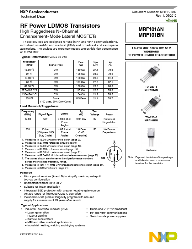
Overview: NXP Semiconductors Technical Data Document Number: MRF101AN Rev. 1, 05/2019 RF Power LDMOS Transistors
High Ruggedness N--Channel Enhancement--Mode Lateral MOSFETs MRF101AN MRF101BN These devices are designed for use in HF and VHF communications, industrial, scientific and medical (ISM) and broadcast and aerospace applications. The devices are extremely rugged and exhibit high performance up to 250 MHz. Typical Performance: VDD = 50 Vdc Frequency (MHz) Signal Type Pout Gps D (W) (dB) (%) 13.56 (1) 27 (2)
40.68 (3) 50 (4)
81.36 (5) 87.5–108 (6,7) 136–174 (7,8)
230 (9) CW CW CW CW CW CW CW Pulse (100 sec, 20% Duty Cycle) 130 CW 125 CW 120 CW 119 CW 130 CW 115 CW 104 CW 115 Peak 27.1 24.9 23.8 22.8 23.2 20.6 21.2 21.1 79.6 79.6 81.5 82.1 80.8 76.8 76.5 76.7 1.8–250 MHz, 100 W CW, 50 V WIDEBAND
RF POWER LDMOS TRANSISTORS
S
GSD TO--220--3 MRF101AN S Load Mismatch/Ruggedness Frequency (MHz) Signal Type VSWR Pin Test (W) Voltage Result 40.68 CW > 65:1 at all 0.64 CW 50 No Device Phase Degradation Angles 230 Pulse > 65:1 at all 1.8 Peak 50 No Device (100 sec, 20% Phase (3 dB Degradation Duty Cycle) Angles Overdrive) 1. Measured in 13.56 MHz reference circuit (page 5). D 2. Measured in 27 MHz reference circuit (page 9). 3. Measured in 40.68 MHz reference circuit (page 13). 4. Measured in 50 MHz reference circuit (page 17). 5. Measured in 81.36 MHz reference circuit (page 21). 6. Measured in 87.5–108 MHz broadband reference circuit (page 25). 7. The values shown are the center band performance numbers G across the indicated frequency range. 8. Measured in 136–174 MHz VHF broadband reference circuit (page 30). 9. Measured in 230 MHz fixture (page 34). S DSG TO--220--3 MRF101BN
Backside Note: Exposed backside of the package
and tab also serves as a source terminal for the transistor.