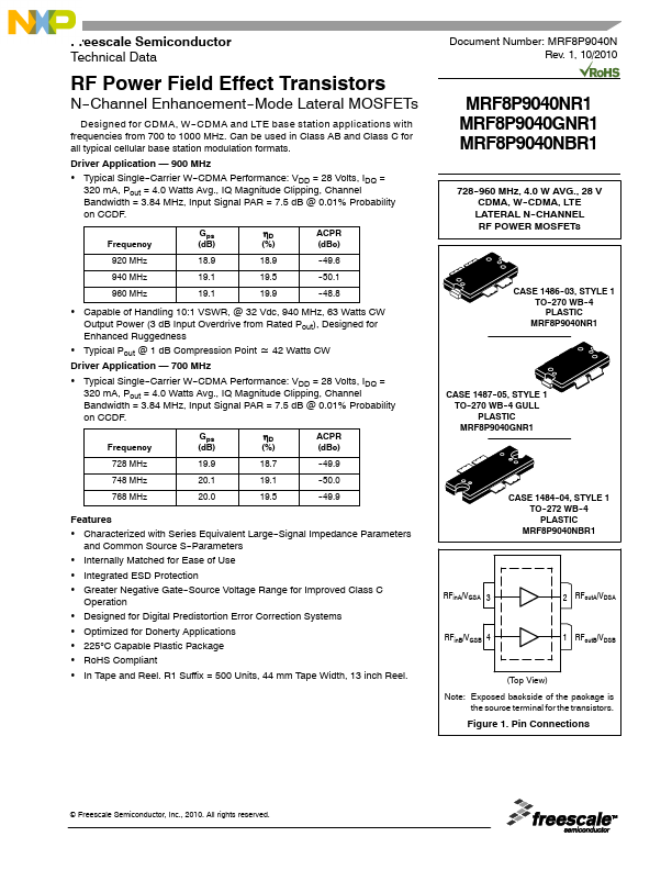
Datasheet4U Logo Datasheet4U.com

MRF8P9040GNR1 - RF Power Field Effect Transistors

Download the MRF8P9040GNR1 datasheet PDF. This datasheet also covers the MRF8P9040NR1 variant, as both devices belong to the same rf power field effect transistors family and are provided as variant models within a single manufacturer datasheet.

Key Features

  • Characterized with Series Equivalent Large--Signal Impedance Parameters and Common Source S--Parameters.
  • Internally Matched for Ease of Use.
  • Integrated ESD Protection.
  • Greater Negative Gate--Source Voltage Range for Improved Class C Operation.
  • Designed for Digital Predistortion Error Correction Systems.
  • Optimized for Doherty.

📥 Download Datasheet

Note: The manufacturer provides a single datasheet file (MRF8P9040NR1-NXP.pdf) that lists specifications for multiple related part numbers.

Full PDF Text Transcription (Reference)

The following content is an automatically extracted verbatim text from the original manufacturer datasheet and is provided for reference purposes only.

View original datasheet text
Freescale Semiconductor Technical Data RF Power Field Effect Transistors N--Channel Enhancement--Mode Lateral MOSFETs Designed for CDMA, W--CDMA and LTE base station applications with frequencies from 700 to 1000 MHz. Can be used in Class AB and Class C for all typical cellular base station modulation formats. Driver Application — 900 MHz • Typical Single--Carrier W--CDMA Performance: VDD = 28 Volts, IDQ = 320 mA, Pout = 4.0 Watts Avg., IQ Magnitude Clipping, Channel Bandwidth = 3.84 MHz, Input Signal PAR = 7.5 dB @ 0.01% Probability on CCDF. Frequency Gps (dB) ηD ACPR (%) (dBc) 920 MHz 940 MHz 960 MHz 18.9 18.9 --49.6 19.1 19.5 --50.1 19.1 19.9 --48.