PHT8N06T
DESCRIPTION
N-channel enhancement mode logic level field-effect power transistor in a plastic envelope suitable for surface mounting. Using ’trench’ technolgy the device features very low on-state resistance and has integral zener diodes giving ESD protection. It is intended for use in DC-DC converters and general purpose switching applications.
QUICK REFERENCE DATA
SYMBOL VDS ID Ptot Tj RDS(ON) PARAMETER Drain-source voltage Drain current Total power dissipation Junction temperature Drain-source on-state resistance VGS = 10 V MAX. 55 7.5 1.8 150 80 UNIT V A W ˚C mΩ
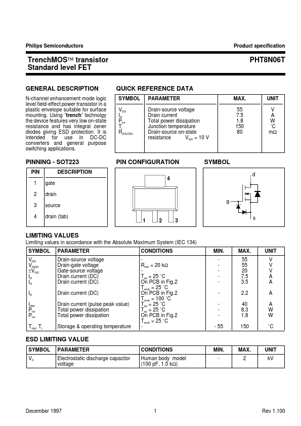
PINNING
- SOT223
PIN 1 2 3 4 gate drain source drain (tab) DESCRIPTION
PIN CONFIGURATION
SYMBOL d g s
LIMITING VALUES
Limiting values in accordance with the Absolute Maximum System (IEC 134) SYMBOL VDS VDGR ±VGS ID ID ID IDM Ptot Ptot Tstg, Tj PARAMETER Drain-source voltage Drain-gate voltage Gate-source voltage Drain current (DC) Drain current (DC) Drain current (DC) Drain current (pulse peak...