Datasheet4U Logo Datasheet4U.com
NXP Semiconductors logo

PLS173 Datasheet

Manufacturer: NXP Semiconductors
PLS173 datasheet preview

Datasheet Details

Part number PLS173
Datasheet PLS173_PhilipsSemiconductors.pdf
File Size 73.50 KB
Manufacturer NXP Semiconductors
Description Programmable logic array
PLS173 page 2 PLS173 page 3

PLS173 Overview

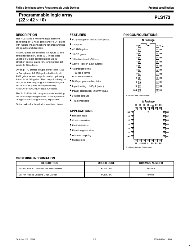
The PLS173 is a two-level logic element consisting of 42 AND gates and 10 OR gates with fusible link connections for programming I/O polarity and direction. All AND gates are linked to 12 inputs (I) and 10 bidirectional I/O lines (B). These yield variable I/O gate configurations via 10 direction control gates (D), ranging from 22 inputs to 10 outputs.

PLS173 Key Features

  • I/O propagation delay: 30ns (max.)
  • 12 inputs
  • 42 AND gates
  • 10 OR gates
  • 10 bidirectional I/O lines
  • Active-High or -Low outputs
  • 42 product terms
  • 32 logic terms
  • 10 control terms
NXP Semiconductors logo - Manufacturer

More Datasheets from NXP Semiconductors

See all NXP Semiconductors datasheets

Part Number Description
PLS100 (PLS100 / PLS101) Programmable logic arrays
PLS101 (PLS100 / PLS101) Programmable logic arrays
PLS105 Field-Programmable Logic Sequencer
PLS155 Programmable Logic Sequencer
PLS159A Programmable logic sequencer 16 x 45 x 12
PLS167 FIELD PROGRAMMABLE LOGIC SEQUENCER
PLS167A FIELD PROGRAMMABLE LOGIC SEQUENCER
PLS168 FIELD PROGRAMMABLE LOGIC SEQUENCER

PLS173 Distributor

Datasheet4U Logo
Since 2006. D4U Semicon. About Datasheet4U Contact Us Privacy Policy Purchase of parts