NXP Semiconductors TDA3617
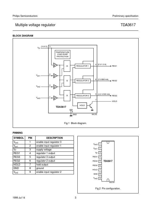
The TDA3617J is a multiple output voltage regulator with three independent regulators.| Part No. | TDA3617 |
|---|---|
| Datasheet | TDA3617 Download |
| Manufacturer |  NXP Semiconductors |
| Description | Multiple voltage regulator |
| Buy | Stock & Price |
FEATURES
General● Three VP-state controlled regulators (regulators 1, 2 and 3)
● Very good stability and noise behaviour
● Separate control pins for switching regulators 1, 2 and 3
● Supply voltage range from −18 to +50 V
● Low quiescent current (when regulators 1, 2 and 3 are switched off)
● High ripple rejection
● Hold output for indicating regulator 1 and/or 2 and/or 3 out of regulation. Protections
● Reverse polarity safe (down to −18 V without high reverse current)
● Able to withstand voltages up to 18 V at the outputs (supply line may be short circuited)
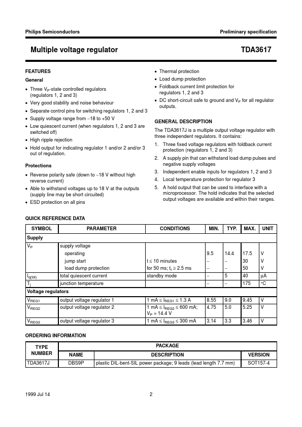
● ESD protection on all pins QUICK REFERENCE DATA SYMBOL Supply VP supply voltage operating jump start load dump protection Iq(tot) Tj VREG1 VREG2 VREG3 total quiescent current junction temperature 1 mA ≤ IREG1 ≤ 1.3 A 1 mA ≤ IREG2 ≤ 600 mA; VP = 14.4 V 1 mA ≤ IREG3 ≤ 300 mA t ≤ 10 minutes for 50 ms; tr ≥ 2.5 ms standby mode 9.5 − − − − 8.55 4.75 3.14 14.4 − − 5 − 9.0 5.0 3.3 PARAMETER CONDITIONS MIN. TYP.
● Thermal protection
●...