NXP Semiconductors TDA4671
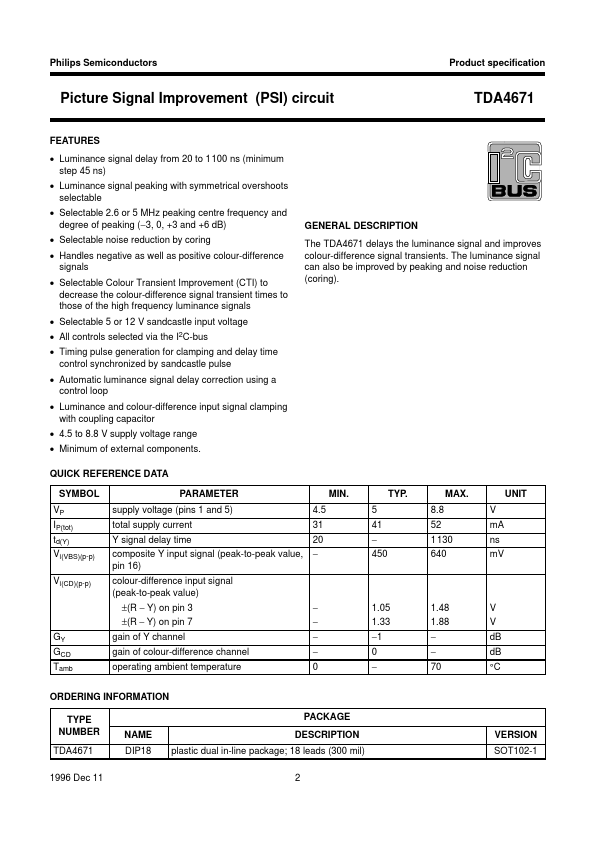
The TDA4671 delays the luminance signal and improves colour-difference signal transients. The luminance signal can also be improved by peaking and noise reduction (coring). handbook, halfpage TDA4671 VP1 1 CDL 2 Vi(R − Y) 3 Vo(R − Y) 4 VP2 5 Vo(B − Y) 6 Vi(B − Y) 7 GND2 8 SDA 9 MED747 18 GND1 17 SAND 16 ViY 15 Cref TDA4671 14 CCLP2 13 CCLP1 12 VoY 11 CCOR 10 SCL 1996 Dec 11 4 Philips Semiconductors Product specification Picture Signal Improvement (PSI) circuit...| Part No. | TDA4671 |
|---|---|
| Datasheet | TDA4671 Download |
| Manufacturer |  NXP Semiconductors |
| Description | Picture Signal Improvement PSI |
| Buy | Stock & Price |
FEATURES
● Luminance signal delay from 20 to 1100 ns (minimum step 45 ns)● Luminance signal peaking with symmetrical overshoots selectable
● Selectable 2.6 or 5 MHz peaking centre frequency and degree of peaking (−3, 0, +3 and +6 dB)
● Selectable noise reduction by coring
● Handles negative as well as positive colour-difference signals
● Selectable Colour Transient Improvement (CTI) to decrease the colour-difference signal transient times to those of the high frequency luminance signals
● Selectable 5 or 12 V sandcastle input voltage
● All controls selected via the I2C-bus
● Timing pulse generation for clamping and delay time control synchronized by sandcastle pulse
● Automatic luminance signal delay correction using a control loop
● Luminance and colour-difference input signal clamping with coupling capacitor
● 4.5 to 8.8 V supply voltage range
● Minimum of external components. QUICK REFERENCE DATA SYMBOL VP IP(tot) td(Y) Vi(VBS)(p-p) Vi(CD)(p-p) PARAMETER supply voltage (pins 1 and...