NXP Semiconductors TDA8752B
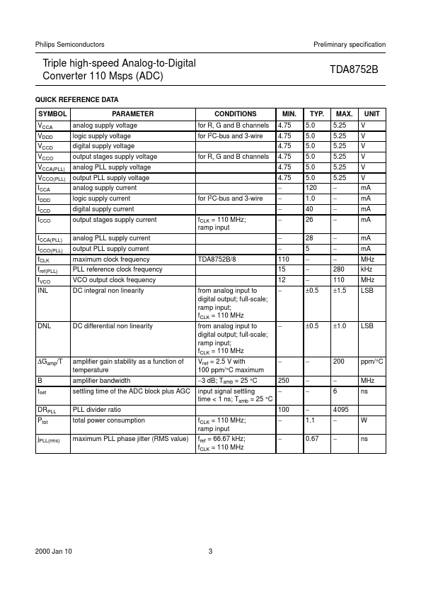
The TDA8752B is a triple 8-bit ADC with controllable amplifiers and clamps for the digitizing of large bandwidth RGB signals. The clamp level, the gain and all of the other settings are controlled via a serial interface (either I2C-bus or 3-wire serial bus, selected via a logic input). The IC also includes a PLL that can be locked to the horizontal line frequency and generates the ADC clock.| Part No. | TDA8752B |
|---|---|
| Datasheet | TDA8752B Download |
| Manufacturer |  NXP Semiconductors |
| Description | Triple high-speed Analog-to-Digital Converter 110 Msps ADC |
| Buy | Stock & Price |

FEATURES
● Triple 8-bit ADC● Sampling rate up to 110 MHz
● IC controllable via a serial interface, which can be either I2C-bus or 3-wire, selected via a TTL input pin
● IC analog voltage input from 0.4 to 1.2 V (p-p) to produce a full-scale ADC input of 1 V (p-p)
● 3 clamps for programming a clamping code between −63.5 and +64 in steps of 1⁄2LSB
● 3 controllable amplifiers: gain controlled via the serial interface to produce a full scale resolution of 1⁄2LSB peak-to-peak
● Amplifier bandwidth of 250 MHz
● Low gain variation with temperature
● PLL, controllable via the serial interface to generate the ADC clock, which can be locked to a line frequency of 15 to 280 kHz
● Integrated PLL divider
● Programmable phase clock adjustment cells
● Internal voltage regulators
● TTL compatible digital inputs and outputs
● Chip enable high-impedance ADC output
● Power-down mode
● Possibility to use up to four ICs in the same system, using the I2C-bus interface, or more, using the 3-wire serial interface
● 1.1 W power dissipation.