NXP Semiconductors TDA8779
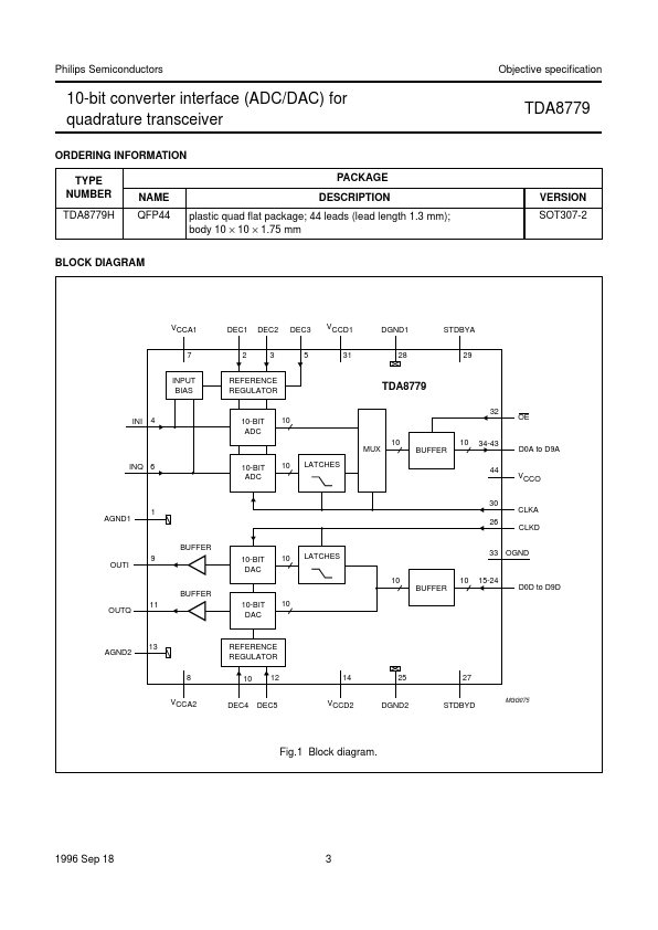
The TDA8779 contains two 10-bit high speed ADCs and two 10-bit DACs for wireless communication (for use in transceiver modules). This device converts two analog input signals (channels I and Q) and digital inputs (D0 to D9) at a maximum sampling rate of 20 MHz. The input bias voltages for the analog input voltages are provided internally at the middle code.| Part No. | TDA8779 |
|---|---|
| Datasheet | TDA8779 Download |
| Manufacturer |  NXP Semiconductors |
| Description | 10-bit converter interface ADC/DAC for quadrature transceiver |
| Buy | Stock & Price |
FEATURES
● Two 10-bit ADCs with multiplexed outputs● Two 10-bit DACs with multiplexed inputs
● Sampling rate for the ADCs and DACs up to 20 MHz
● Digital outputs (for the ADC) and inputs (for the DAC) are TTL/CMOS compatible (2.7 to 5.5 V)
● Internal reference voltage regulator
● Power dissipation 520 mW
● Standby mode.
APPLICATIONS
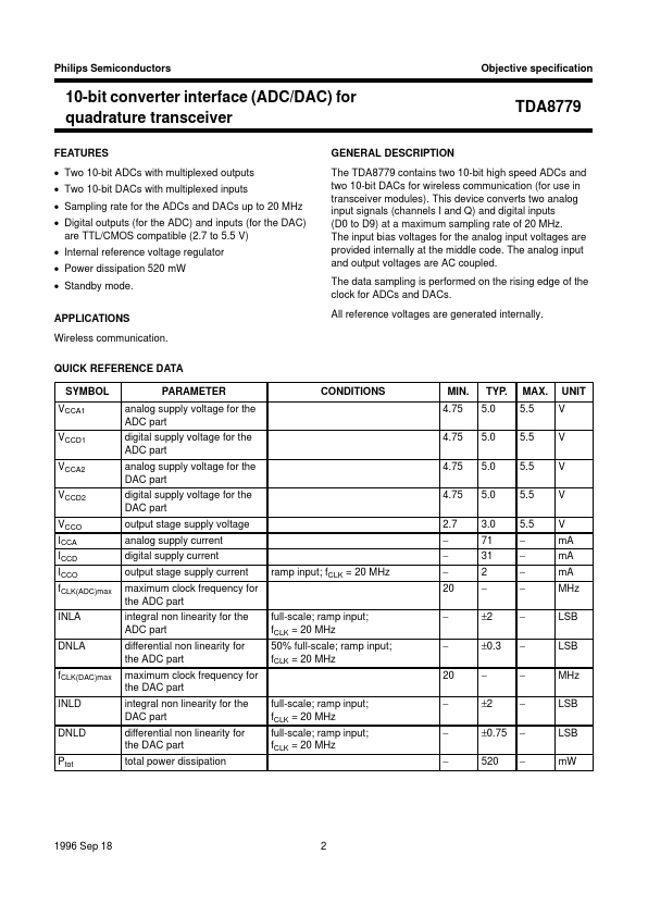
Wireless communication. QUICK REFERENCE DATA SYMBOL VCCA1 VCCD1 VCCA2 VCCD2 VCCO ICCA ICCD ICCO fCLK(ADC)max INLA DNLA fCLK(DAC)max INLD DNLD Ptot PARAMETER analog supply voltage for the ADC part digital supply voltage for the ADC part analog supply voltage for the DAC part digital supply voltage for the DAC part output stage supply voltage analog supply current digital supply current output stage supply current maximum clock frequency for the ADC part integral non linearity for the ADC part differential non linearity for the ADC part maximum clock frequency for the DAC part integral non linearity for the DAC part differential non linearity for the DAC par...