NXP Semiconductors TDA9962
The TDA9962 is a 12-bit analog-to-digital interface for CCD cameras. The device includes a correlated double sampling circuit, PGA, clamp loops and a low-power 12-bit ADC together with its reference voltage regulator. The PGA gain and the ADC input clamp level are controlled via the serial interface.| Part No. | TDA9962 |
|---|---|
| Datasheet | TDA9962 Download |
| Manufacturer |  NXP Semiconductors |
| Description | 12-bit/ 3.0 V/ 20 Msps analog-to-digital interface for CCD cameras |
| Buy | Stock & Price |
FEATURES
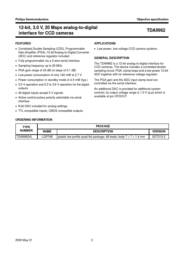
● Correlated Double Sampling (CDS), Programmable Gain Amplifier (PGA), 12-bit Analog-to-Digital Converter (ADC) and reference regulator included● Fully programmable via a 3-wire serial interface
● Sampling frequency up to 20 MHz
● PGA gain range of 24 dB (in steps of 0.1 dB)
● Low power consumption of only 140 mW at 2.7 V
● Power consumption in standby mode of 4.5 mW (typ.)
● 3.0 V operation and 2.2 to 3.6 V operation for the digital outputs
● All digital inputs accept 5 V signals
● Active control pulses polarity selectable via serial interface
● 8-bit DAC included for analog settings
● TTL compatible inputs, CMOS compatible outputs. ORDERING INFORMATION TYPE NUMBER TDA9962HL PACKAGE NAME LQFP48
DESCRIPTION
plastic low profile quad flat package; 48 leads; body 7 × 7 × 1.4 mmAPPLICATIONS
TDA9962● Low-power, low-voltage CCD camera systems.
GENERAL DESCRIPTION
An additional DAC is provided for additional system controls; its output voltage range is 1.0 V (p-p) which is available at pin OFDOUT.