N02L083WC2A Overview
Key Specifications
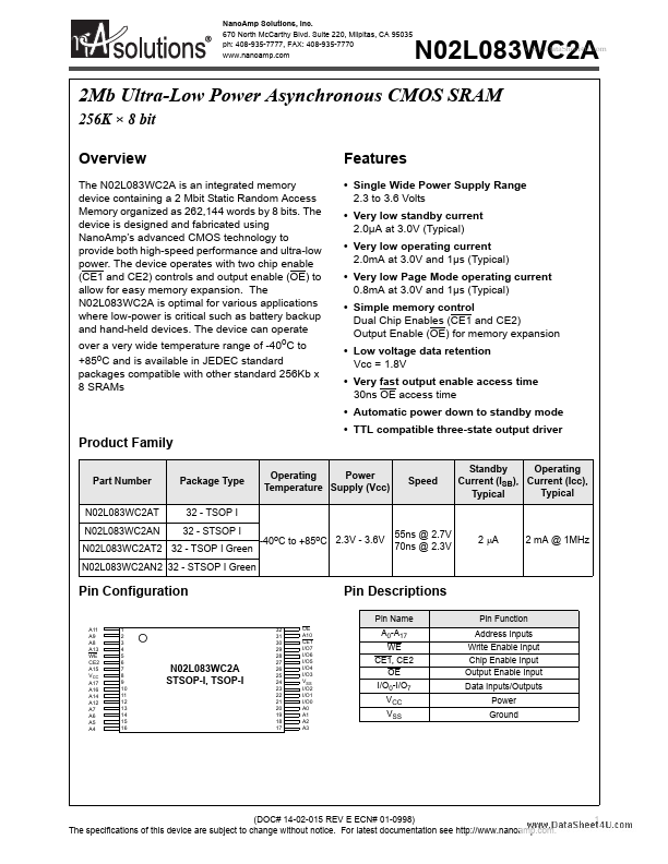
Package: LSSOP
Operating Voltage: 3 V
Max Voltage (typical range): 3.6 V
Min Voltage (typical range): 2.3 V
Key Features
- Single Wide Power Supply Range 2.3 to 3.6 Volts
- Very low standby current 2.0µA at 3.0V (Typical)
- Very low operating current 2.0mA at 3.0V and 1µs (Typical)
- Very low Page Mode operating current 0.8mA at 3.0V and 1µs (Typical)
- Simple memory control Dual Chip Enables (CE1 and CE2) Output Enable (OE) for memory expansion
- Low voltage data retention Vcc = 1.8V
- Very fast output enable access time 30ns OE access time
- Automatic power down to standby mode