Datasheet4U Logo Datasheet4U.com

NT5CC1024M4BN - 4Gb DDR3 SDRAM B-Die

Download the NT5CC1024M4BN datasheet PDF. This datasheet also covers the NT5CB variant, as both devices belong to the same 4gb ddr3 sdram b-die family and are provided as variant models within a single manufacturer datasheet.

📥 Download Datasheet

Note: The manufacturer provides a single datasheet file (NT5CB-1024M.pdf) that lists specifications for multiple related part numbers.

Datasheet Details

Part number NT5CC1024M4BN
Manufacturer Nanya
File Size 2.64 MB
Description 4Gb DDR3 SDRAM B-Die
Datasheet download datasheet NT5CC1024M4BN Datasheet

General Description

The 4Gb Double-Data-Rate-3 (DDR3) DRAMs is a high-speed CMOS Double Data Rate32 SDRAM containing 4,294,967,296 bits.

It is internally configured as an octal-bank DRAM.

The 4Gb chip is organized as 128Mbit x 4 I/O x 8 bank , 64Mbit x 8 I/O x 8 banks and 32Mbit x16 I/O x 8 banks.

Overview

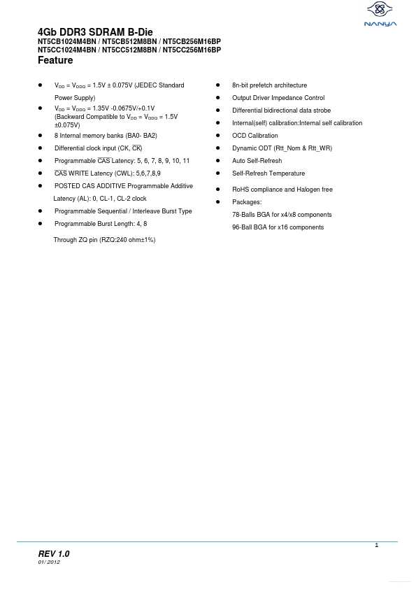
4Gb DDR3 SDRAM B-Die NT5CB1024M4BN / NT5CB512M8BN / NT5CB256M16BP NT5CC1024M4BN / NT5CC512M8BN / NT5CC256M16BP Feature  VDD = VDDQ = 1.5V ± 0.075V (JEDEC Standard Power Supply)  VDD = VDDQ = 1.35V -0.0675V/+0.1V (Backward Compatible to VDD = VDDQ = 1.5V ±0.075V) 8 Internal memory banks (BA0- BA2) Differential clock input (CK, ) Programmable Latency: 5, 6, 7, 8, 9, 10, 11  WRITE Latency (CWL): 5,6,7,8,9 POSTED CAS ADDITIVE Programmable Additive Latency (AL): 0, CL-1, CL-2 clock   Programmable Sequential / Interleave Burst Type Programmable Burst Length: 4, 8 Through ZQ pin (RZQ:240 ohm±1%)           8n-bit prefetch architecture Output Driver Impedance Control Differential bidirectional data strobe Internal(self) calibration:Internal self calibration OCD Calibration Dynamic ODT (Rtt_Nom & Rtt_WR) Auto Self-Refresh Self-Refresh Temperature RoHS compliance and Halogen free Packages: 78-Balls BGA for x4/x8 components 96-Ball BGA for x16 components      1 REV 1.0 01/ 2012 Free Datasheet http://www.0PDF.

Key Features

  • and all of the control and address inputs are synchronized with a pair of externally supplied differential clocks. Inputs are latched at the cross point of differential clocks (CK rising and  falling). All I/Os are synchronized with a single ended DQS or differential DQS pair in a source synchronous fashion. These devices operate with a single 1.5V ± 0.075V and 1.35V -0.0675V/+0.1V power supply and are available in BGA packages. 2 REV 1.0 01/ 2012 Free Datasheet http://www.0PDF. com 4Gb DDR.