Datasheet4U Logo Datasheet4U.com

NT5TU64M8DE - 512Mb DDR2 SDRAM

Description

The 512Mbit Double-Data-Rate-2 (DDR2) DRAMs is a high-speed CMOS Double Data Rate 2 SDRAM containing 536,870,912 bits.

It is internally configured as a quad-bank DRAM.

The 512Mb chip is organized as 16Mbit x 8 I/O x 4 bank or 8Mbit x 16 I/O x 4 bank device.

Features

  • (1) posted CAS with additive latency, (2) write latency = read latency -1, (3) normal and weak strength data-output driver, (4) variable data-output impedance adjustment and (5) an ODT (On-Die Termination) function. All of the control and address inputs are synchronized with a pair of externally supplied differential clocks. Inputs are latched at the cross point of differential clocks (CK rising and CK falling). All I/Os are synchronized with a single ended DQS or differential DQS pair in a sou.

📥 Download Datasheet

Datasheet preview – NT5TU64M8DE

Datasheet Details

Part number NT5TU64M8DE
Manufacturer Nanya
File Size 2.35 MB
Description 512Mb DDR2 SDRAM
Datasheet download datasheet NT5TU64M8DE Datasheet
Additional preview pages of the NT5TU64M8DE datasheet.
Other Datasheets by Nanya

Full PDF Text Transcription

Click to expand full text
NT5TU64M8DE / NT5TU32M16DG 512Mb DDR2 SDRAM                                        Feature 
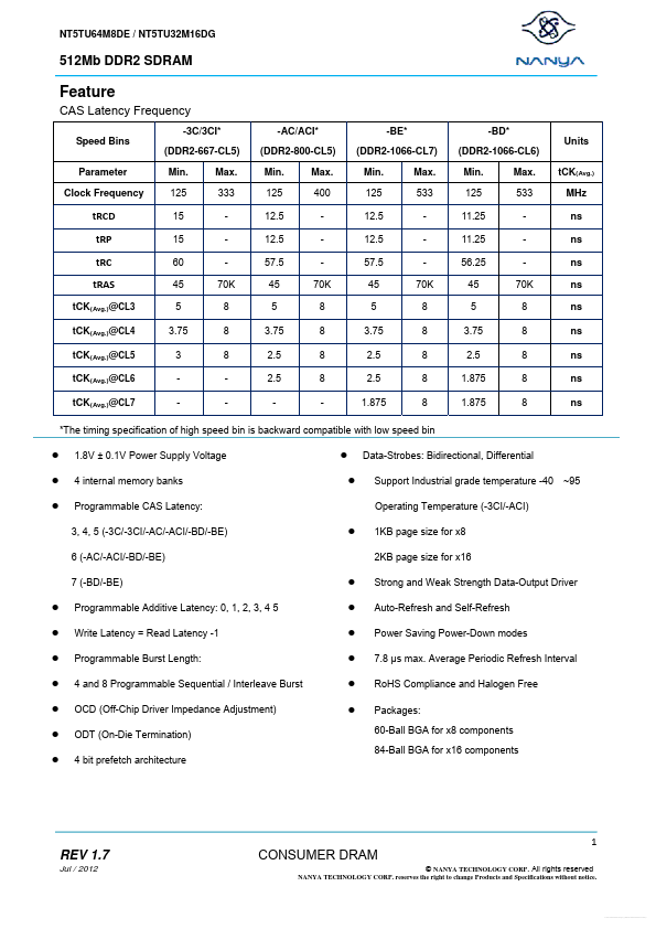
CAS Latency Frequency -3C/3CI* Speed Bins (DDR2-667-CL5) Parameter Clock Frequency Min. 125 15 15 60 45 5 3.75 3 Max. 333 70K 8 8 8 (DDR2-800-CL5) Min. 125 12.5 12.5 57.5 45 5 3.75 2.5 2.5 Max. 400 70K 8 8 8 8 (DDR2-1066-CL7) Min. 125 12.5 12.5 57.5 45 5 3.75 2.5 2.5 1.875 Max. 533 70K 8 8 8 8 8 (DDR2-1066-CL6) Min. 125 11.25 11.25 56.25 45 5 3.75 2.5 1.875 1.875 Max. 533 70K 8 8 8 8 8 tCK(Avg.) MHz ns ns ns ns ns ns ns ns ns -AC/ACI* -BE* -BD* Units tRCD  tRP  tRC  tRAS  tCK(Avg.)@CL3  tCK(Avg.)@CL4 tCK(Avg.)@CL5 tCK(Avg.)@CL6 tCK(Avg.)@CL7 *The timing specification of high speed bin is backward compatible with low speed bin z z z 1.8V ± 0.
Published: |