National Semiconductor 100310
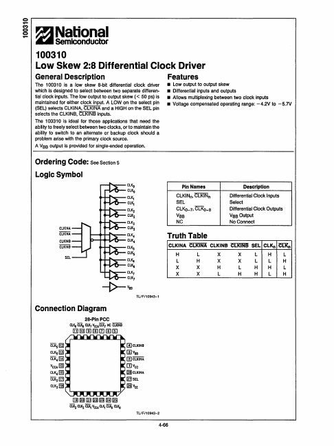
The 100310 is a low skew a·bit differential clock driver which is designed to select between two separate differen· tial clock inputs. The low output to output skew « 50 ps) is maintained for either clock input. The 100310 is ideal for those applications that need the ability to freely select between two clocks.| Part No. | 100310 |
|---|---|
| Datasheet | 100310 Download |
| Manufacturer |  National Semiconductor |
| Description | Low Skew 2:8 Differential Clock Driver |
| Buy | Stock & Price |
GENERAL DESCRIPTION
A LOW on the select pin (SEL) selects CLKINA. CLKINA and a HIGH on the SEl pin selects the CLKINS. ClKINS inputs. or to maintain the ability to switch to an alternate or backup clock should a problem arise with the primary clock source. A Vss output is provided for single-ended operation.FEATURES
● Low output to output skew● Differential inputs and outputs
● Allows multiplexing between two clock inputs
● Voltage compensated operating range: -4.2V to -5.7V Ordering Code: See Section 5 Logic Symbol CLKINA ClKINA CLKINB CLKINB SEL ClKg CLKg CLKj CLKj CLK2 CLK2 ClK3 CLK3 CLK. CLK. CLKs CLKs CLKs CLKs ClK7 CLK7 --t>--vss Tl/F/10943-1 Connection Diagram 28-Pln pcc rn ClKe ClKe ax7VCCAax7 NC ClKINB [TI [Q] [!] [l][IIIII Pin Names CLKINn● ClKINn SEL CLKo_7. CD<o-a Vss NC
DESCRIPTION
Differential Clock Inputs Select Differential Clock Outputs Vss Output No Connect Truth Table ClKINA ClKINA ClKINB ClKINB SEl ClKn C[Kn H L X X LH L l H X X LL H X X H L HH L X X L H HL H ClKs...
