Datasheet4U Logo Datasheet4U.com

100311 - Low Skew 1:9 Differential Clock Driver

General Description

clocks from a single differential input (ClKIN, ClKIN).

used to drive the remaining input line.

Key Features

  • low output to output skew.
  • 2000V ESD protection II 1:9 low skew clock driver II Differential inputs and outputs Ordering Code: See Section 5 Logic Symbol - -CLKo CLKo ClK1 CLK1 ClK2 CLK2 ClK3 CLK3 ClKIN ---r+-I~- ClK. ClKIN CLK. EN CLKs CLK5 ClK& CLK& ClK7 CLK7 L+-- C l Ks CLKs --(>-Vee TL/F/l0648-1 Connection Diagram 28-Pln pee eLKs aRs CLK7 Vo:J. W.

📥 Download Datasheet

Full PDF Text Transcription (Reference)

The following content is an automatically extracted verbatim text from the original manufacturer datasheet and is provided for reference purposes only.

View original datasheet text
o ~----------------------------------------------------------------------------~ ~ ~National ow ~ ~ Semiconductor ~ 100311 Low Skew 1:9 Differential Clock Driver General Description 
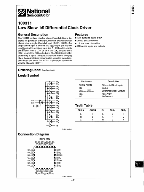
The 100311 contains nine low skew differential drivers, de- signed for generation of multiple, minimum skew differential clocks from a single differential input (ClKIN, ClKIN). If a single-ended input is desired, the VBB output pin may be used to drive the remaining input line. A HIGH on the enable run pin (EN) will force a lOW on all of the ClKn outputs and a HIGH on all of the output pins. The 100311 is ideal for distributing a signal throughout a system without worrying about the original signal becoming too corrupted by undesir- able delays and skew.