GENERAL DESCRIPTION
ABSOLUTE MAXIMUM RATINGS
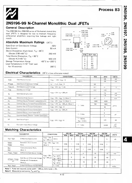
(25°o Gate-Drain or Gate-Source Voltage Gate Current Device Dissipation (Each Side), T/\ = 85°C (Derate 2.56 mW/°C) -50V 50 mA 250 mW Total Device Dissipation, Ta = 85°C (Derate 4.3 mW/°C) 500 mW Storage Temperature Range Lead Temperature (1/16" from case for 10 seconds) 65°Cto+200°C a 300 C 0175- 0195 " (4445 -4.9531 0.209 0.230 (5.309 SM2! 0170-0.210 (4.318 5T334) SLATIMG PLANE mnr 016 -0 019 ddq] 0.030 PIN FET (12) 1 SI 2 D1 3 G1 5 S2 6 D2 7 G2 0.028-0.048 ELECTRICAL CHARACTERISTICS
(25°c unless otherwise noted) PARAMETER CONDITIONS V GS - -30V, Vds-0 BVqsS v GS(off) Vqs Gate-Source Breakdown Voltage Gate-Source Cutoff Voltage Gate-Source Voltage Gl - -lilA, V DS -0 VDS" 20V, Dl - 1 nA V DG - 20V, Dl - 200 jiA iDSS 9fs gfs gos gos C, ss C rss NF Saturation Drain Current Common-Source Forward Transconductance Common-Source Forward Transconductance Common-Source Output Conductance Common-Source Output Conductance Common-Source Input Capacit... National Semiconductor