GENERAL DESCRIPTION
ABSOLUTE MAXIMUM RATINGS
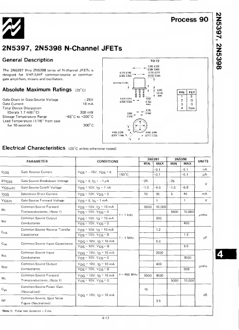
(25°o Gate-Drain or Gate-Source Voltage Gate Current Total Device Dissipation (Derate 1.7 mW/°C) Storage Temperature Range Lead Temperature (1/16" from case for 10 seconds) -25V 10mA 300 mW -65° C to +200°C 300° C OJ 75-0 . 196 "' [4.445-4.953) SEATIMG PLANE 19.496-0.483) TO-72 _ Q.209-0.230 T I57309~5.8«) 0.179-0.210 In. 318-5.334) L - (12.70) f MIN 9.10O ~(2~540) 0.936-Q.946 yj;>/>~_^^ 0.028-0.048 (0l914-1.1fi«)X..- y '/ y (oTl1-1.219) PIN FET 1 S 2 D 3 G 4 Case ELECTRICAL CHARACTERISTICS
(25c un less otherwise noted) 'GSS SVgss ^GS(off) IDSS VGS(f) 9fs Cj ss 9fs ps NF PARAMETER Gate Reverse Current Gate-Source Breakdown Voltage Gate-Source Cutoff Voltage Saturation Drain Current Gate-Source Forward Voltage Common-Source Forward Transconductance, (Note 1) Common-Source Output Conductance Common-Source Reverse Transfer Capacitance Common-Source Input Capacitance Common-Source Input Conductance Common-Source Output Conductance Common-Source Forward Transconductance, (Note 1) Common-Source Power Gain (Neutralized! National Semiconductor