GENERAL DESCRIPTION
ABSOLUTE MAXIMUM RATINGS
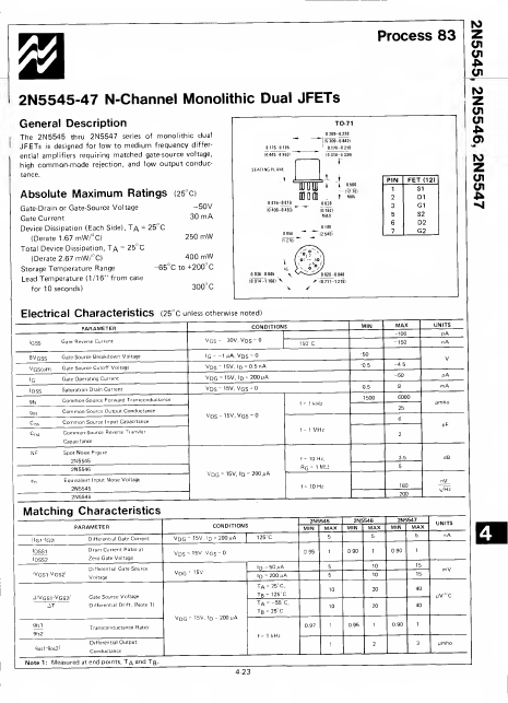
(250 Gate-Drain or Gate-Source Voltage Gate Current -50V 30 mA Device Dissipation (Each Side), Ta = 25°C (Derate 1.67mW/°C) 250 mW Total Device Dissipation, Ta = 25 C (Derate 2.67 mW/°C) 400 mW Storage Temperature Range -65°C to +200 C Lead Temperature (1/16" from case for 10 seconds) 300° C TO-71 Q.2D9- 0.230 ""*" 1(5-309- 5.8421 0175 0.195 ! Q.170 -0.210 (4.445-4.953) (4318 -5334) SEATING PLANE D. 016-0019 r t HJUUJ i mom 0.030 t » 0.500 - n.m ( | MM io.4O6-0.4B3t ~0.762) MAX 0.100 0050 ~" """'(25401 *~" (U70t "~* ~ M /^f>\ i ( 01 V S S 036 0.G46 V (0.914-1.168) y ^^—^-^0028 -0.048 / 10711-1.219) \● Process 83 z 01 01 01 z10 01 01 j^ P z PIN FET (12) 01 1 S1 01 2 D1 3 G1 5 S2 6 D2 7 G2 ELECTRICAL CHARACTERISTICS
(25'c unless otherwise noted) PARAMETER Gate Reverse Current CONDITIONS V G S- 30V,V DS -0 BVGSS v GS(off) Gate-Source Breakdown Voltage Gate-Source Cutoff Voltage Gate Operating Current 9fs 9os Cj ss Saturation Drain Current Commo... National Semiconductor