Description
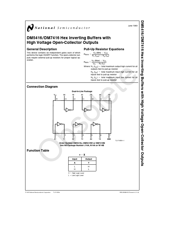
This device contains six independent gates each of which performs the logic INVERT function The open-collector outputs require external pull-up resistors for proper logical operation Pull-Up Resistor Equations RMAX e VO (Min) b VOH N1 (IOH) a N2 (IIH) RMIN e VO (Max) b VOL IOL b N3 (IIL) Where N1 (IOH) e total maximum output high current for all outputs tied to pull-up resistor N2 (IIH) e total maximum input high current for all inputs tied to pull-up resistor N3 (IIL) e total maximum input low current for all inputs tied to pull-up resistor Connection Diagram Dual-In-Line Package Function Table Order Number DM5416J DM5416W or DM7416N See NS Package Number J14A N14A or W14B YeA Input Output AY LH HL H e High Logic Level L e Low Logic Level TL F 6504 – 1 C1995 National Semiconductor Corporation TL F 6504 RRD-B30M105 Printed in U S A Obsolete If Military Aerospace specified devices are required please contact the National Semiconductor Sales Office Distributors for availability and specifications Supply Voltage 7V Input Voltage 5 5V Output Voltage 15V Operating Free Air Temperature Range DM54 b55 C to a125 C DM74 0 C to a70 C Storage Temperature Range b65 C to a150 C Note The ‘‘ Remended Operating Conditions Symbol VCC VIH VIL VOH IOL TA Parameter Supply Voltage High Level Input Voltage Low Level Input Voltage High Level Output Voltage Low Level Output Current Free Air Operating Temperature Min 45 2 b55 DM5416 Nom 5 Max 55 08 15 30 125 Min 4 75 2 0 DM7416 Nom 5 Max 5 25 08 15 40 70 Units V V V V mA C Symbol Parameter Conditions Typ Min Max Units (Note 1) VI ICEX VOL II Input Clamp Voltage High Level Output Current Low Level Output Voltage Input Current Max Input Voltage VCC e Min II e b12 mA VCC e Min VO e 15V VIL e Max VCC e Min IOL e Max VIH e Min IOL e 16 mA VCC e Min VCC e Max VI e 5 5V b1 5 250 07 04 1 V mA V mA IIH IIL ICCH High Level Input Current Low Level Input Current Supply Current with Outputs High VCC e Max VI e 2 4V VCC e Max VI e 0 4V VCC e Max 40 b1 6 mA mA 30 48 mA ICCL Supply Current with Outputs Low VCC e Max 27 51 mA Switching Characteristics at VCC e 5V and TA e 25 C (See Section 1 for Test Waveforms and Output Load) Symbol Parameter Conditions Min Max Units tPLH Propagation Delay Time Low to High Level Output CL e 15 pF RL e 110X tPHL Propagation Delay Time High to Low Level Output 15 ns 23 ns Note 1 All typicals are at VCC e 5V TA e 25 C 2 Obsolete Physical Dimensions inches (millimeters) 14-Lead Ceramic Dual-In-Line Package (J) Order Number DM5416J NS Package Number J14A 14-Lead Molded Dual-In-Line Package (N) Order Number DM7416N NS Package Number N14A 3 DM5416 DM7416 Hex Inverting Buffers with High Voltage Open-Collector Outputs Obsolete Physical Dimensions inches (millimeters) (Continued) 14-Lead Ceramic Flat Package (W) Order Number DM5416W NS Package Number W14B LIFE SUPPORT POLICY NATIONAL’S PRODUCTS ARE NOT AUTHORIZED FOR USE AS CRITICAL PONENTS IN LIFE SUPPORT DEVICES OR SYSTEMS WITHOUT THE EXPRESS WRITTEN APPROVAL OF THE PRESIDENT OF NATIONAL SEMICONDUCTOR CORPORATION As used herein 1 Life support devices or systems are devices or systems which (a) are intended for surgical implant into the body or (b).