National Semiconductor 54AC10
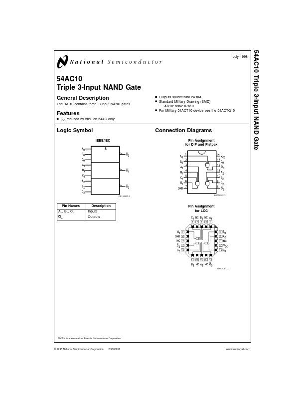
the 54ACTQ10 Features n ICC reduced by 50% on 54AC only Logic Symbol IEEE/IEC Connection Diagrams Pin Assignment for DIP and Flatpak DS100261-1 DS100261-3 Pin Names An, Bn, Cn On Description Inputs Outputs Pin Assignment for LCC DS100261-2 FACT™ is a trademark of Fairchild Semiconductor Corporation. The databook specifications should be met, without exception, to ensure that the system design is reliable over its power supply, temperature, and output/input loading variables.
| Part No. |
54AC10 |
| Datasheet |
54AC10
Download
|
| Manufacturer |
 National Semiconductor |
| Description |
Triple 3-Input NAND Gate |
| Buy |
Stock & Price
|
GENERAL DESCRIPTION
The ’AC10 contains three, 3-input NAND gates. n Outputs source/sink 24 mA n Standard Military Drawing (SMD) — ’AC10: 5962-87610 n For Military 54ACT10 device see © 1998 National Semiconductor Corporation DS100261 ABSOLUTE MAXIMUM RATINGS
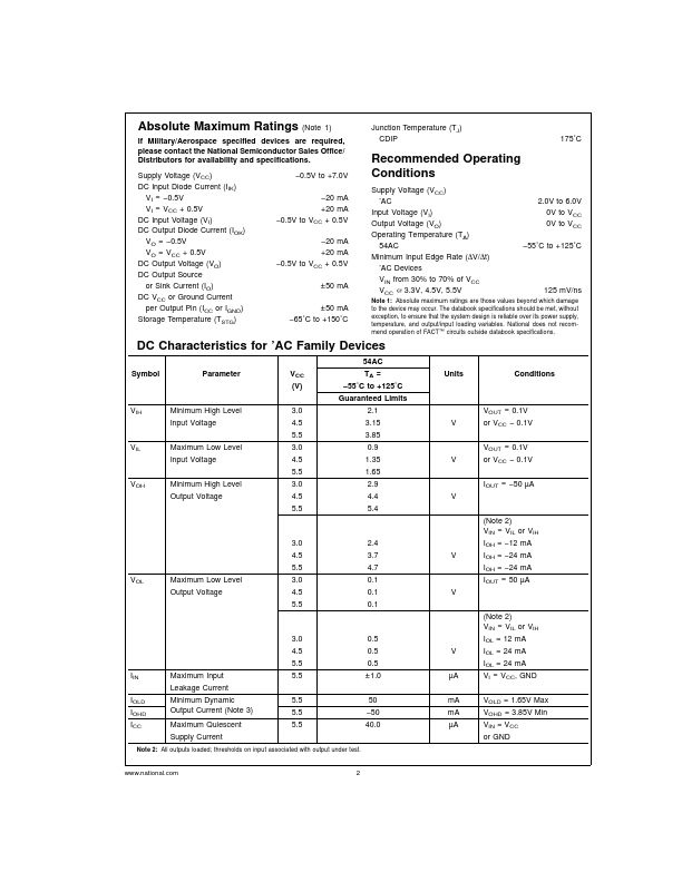
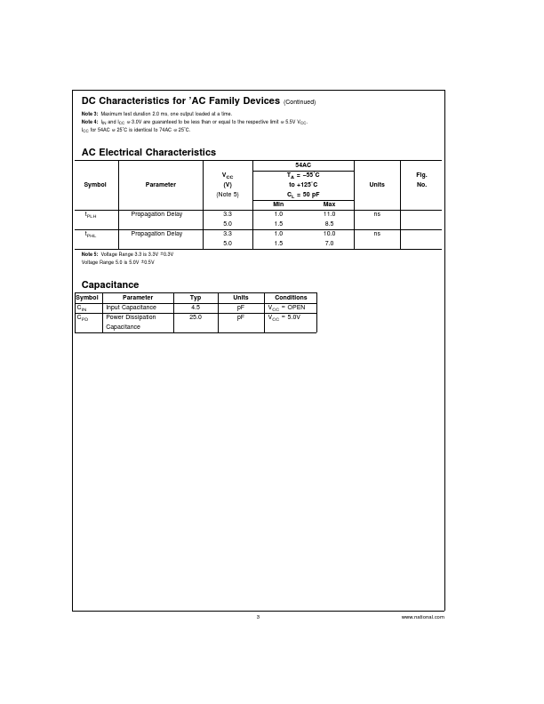
(Note 1) If Military/Aerospace specified devices are required, please contact the National Semiconductor Sales Office/ Distributors for availability and specifications. Supply Voltage (VCC) DC Input Diode Current (IIK) VI = −0.5V VI = VCC + 0.5V DC Input Voltage (VI) DC Output Diode Current (IOK) VO = −0.5V VO = VCC + 0.5V DC Output Voltage (VO) DC Output Source or Sink Current (IO) DC VCC or Ground Current per Output Pin (ICC or IGND) Storage Temperature (TSTG) −0.5V to +7.0V −20 mA +20 mA −0.5V to VCC + 0.5V −20 mA +20 mA −0.5V to VCC + 0.5V Junction Temperature (TJ) CDIP 175˚C Recommended Operating Conditions Supply Voltage (VCC) ’AC Input Voltage (VI) Output Voltage (VO) Operating Temperature (TA) 54AC Minimum Input Edge Rate (∆...