54AC273
Description
The ’273 has eight edge-triggered D-type flip-flops with individual D inputs and Q outputs.
Key Features
- n n n n n n n n n
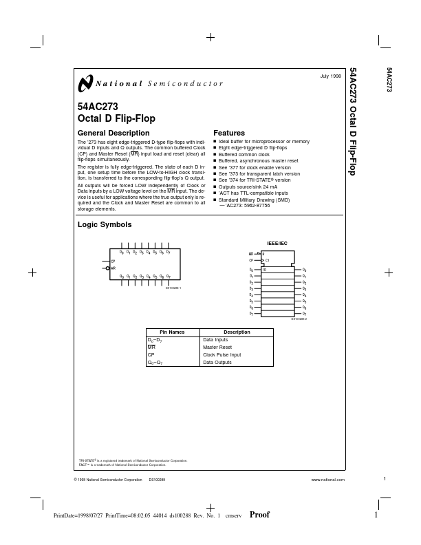
The ’273 has eight edge-triggered D-type flip-flops with individual D inputs and Q outputs.