GENERAL DESCRIPTION
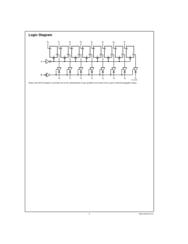
When LE is LOW, the data that meets the setup time is latched. Data appears on the bus when the Output Enable (OE) is LOW. When OE is HIGH, the bus output is in the high impedance state. FEATURES
n n n n n n ICC and IOZ reduced by 50% Eight latches in a single package TRI-STATE outputs for bus interfacing Outputs source/sink 24 mA ’ACT373 has TTL-compatible inputs Standard Microcircuit Drawing (SMD) — ’AC373: 5962-87555 — ’ACT373: 5962-87556 Logic Symbols IEEE/IEC DS100329-1 DS100329-2 Pin Names D0–D7 LE OE O0–O7 DESCRIPTION
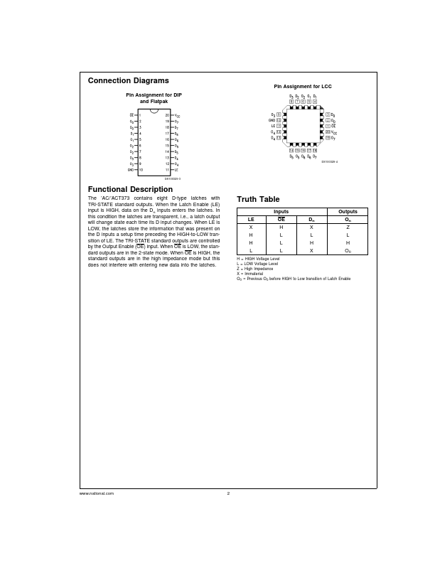
Data Inputs Latch Enable Input Output Enable Input TRI-STATE Latch Outputs TRI-STATE ® is a registered trademark of National Semiconductor Corporation. FACT ® is a registered trademark of Fairchild Semiconductor Corporation. © 1998 National Semiconductor Corporation DS100329 Connection Diagrams Pin Assignment for DIP and Flatpak Pin Assignment for LCC DS100329-4 DS100329-3 Functional DESCRIPTION
The ’AC/’ACT373 contains eight D-type latches with TRI-STATE standard outputs. National Semiconductor