54ACT109
54ACT109 is Dual JK Positive Edge-Triggered Flip-Flop manufactured by National Semiconductor.
- Part of the 54AC109 comparator family.
- Part of the 54AC109 comparator family.
..
54AC109
- 54ACT109 Dual JK Positive Edge-Triggered Flip-Flop
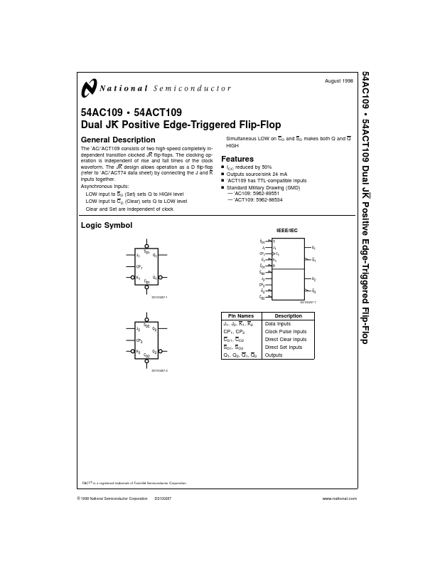
August 1998
54AC109
- 54ACT109 Dual JK Positive Edge-Triggered Flip-Flop
General Description
The ’AC/’ACT109 consists of two high-speed pletely independent transition clocked JK flip-flops. The clocking operation is independent of rise and fall times of the clock waveform. The JK design allows operation as a D flip-flop (refer to ’AC/’ACT74 data sheet) by connecting the J and K inputs together. Asynchronous Inputs: LOW input to SD (Set) sets Q to HIGH level LOW input to CD (Clear) sets Q to LOW level Clear and Set are independent of clock Simultaneous LOW on CD and SD makes both Q and Q HIGH
Features n...