54ACT175
54ACT175 is Quad D Flip-Flop manufactured by National Semiconductor.
- Part of the 54AC175 comparator family.
- Part of the 54AC175 comparator family.
Description
The ’AC/’ACT175 is a high-speed quad D flip-flop. The device is useful for general flip-flop requirements where clock and clear inputs are mon. The information on the D inputs is stored during the LOW-to-HIGH clock transition. Both true and plemented outputs of each flip-flop are provided. A Master Reset input resets all flip-flops, independent of the Clock or D inputs, when LOW. n n n n n n Buffered positive edge-triggered clock Asynchronous mon reset True and plement output Outputs source/sink 24 m A ’ACT175 has TTL-patible inputs Standard Microcircuit Drawing (SMD)
- ’AC175: 5962-89552
- ’ACT175: 5962-89693
Features n Edge-triggered D-type inputs
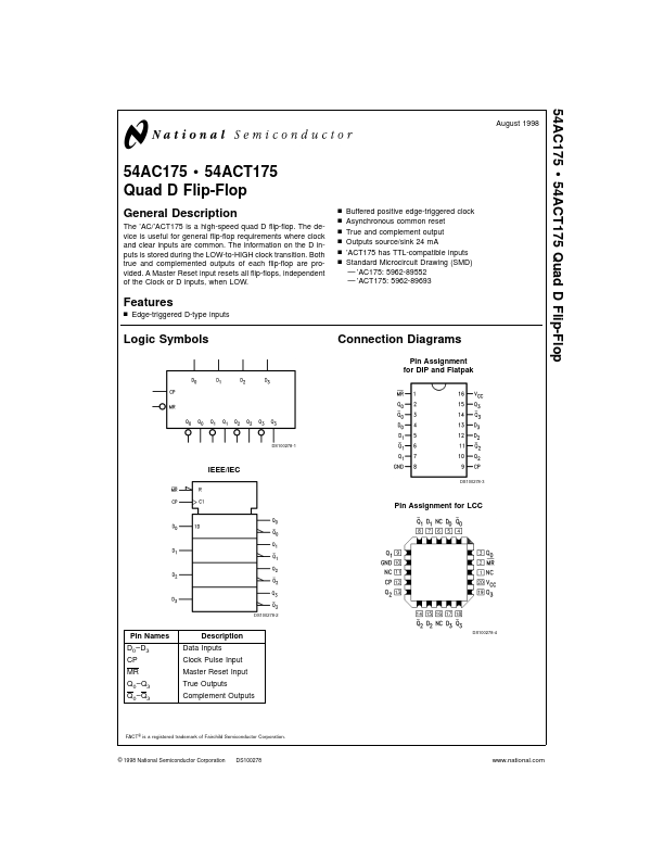
Logic Symbols
Connection Diagrams
Pin Assignment for DIP and Flatpak
DS100278-1
IEEE/IEC
DS100278-3
Pin Assignment for LCC
DS100278-2
Pin Names D0- D3 CP MR Q0- Q3 Q0- Q3
Description
Data Inputs Clock Pulse Input Master Reset Input True Outputs plement Outputs
DS100278-4
FACT ® is a registered trademark of Fairchild Semiconductor Corporation.
© 1998 National Semiconductor Corporation
DS100278
.national.
Functional Description
The ’AC/’ACT175 consists of four edge-triggered D flip-flops with individual D inputs and Q and Q outputs. The Clock and Master Reset are mon. The four flip-flops will store the state of their individual D inputs on the LOW-to-HIGH clock (CP) transition, causing individual Q and Q outputs to follow. A LOW input on the Master Reset (MR) will force all Q outputs LOW and Q outputs HIGH independent of Clock or Data inputs. The ’AC/’ACT175 is useful for general logic applications where a mon Master Reset and Clock are acceptable.
Truth Table
Inputs
@ tn, MR = H
Outputs
@ tn+1
Dn L H
H = HIGH Voltage Level L = LOW Voltage Level tn = Bit Time before Clock Pulse tn+1 = Bit Time after Clock Pulse
Qn L H
Qn H L
Logic Diagram
DS100278-5
Please note that this diagram is provided only for the understanding of logic operations and should not be used to estimate propagation...