54ACT299
54ACT299 is 8-Input Universal Shift/Storage Register manufactured by National Semiconductor.
- Part of the 54AC299 comparator family.
- Part of the 54AC299 comparator family.
Description
The ’AC/’ACT299 is an 8-bit universal shift/storage register with TRI-STATE ® outputs. Four modes of operation are possible: hold (store), shift left, shift right and load data. The parallel load inputs and flip-flop outputs are multiplexed to reduce the total number of package pins. Additional outputs are provided for flip-flops Q0, Q7 to allow easy serial cascading. A separate active LOW Master Reset is used to reset the register. n mon parallel I/O for reduced pin count n Additional serial inputs and outputs for expansion n Four operating modes: shift left, shift right, load and store n TRI-STATE outputs for bus-oriented applications n Outputs source/sink 24 m A n ’ACT299 has TTL-patible inputs n Standard Microcircuit Drawing (SMD) ’AC299: 5962-88754 ’ACT299: 5962-88771
Features n ICC and IOZ reduced by 50%
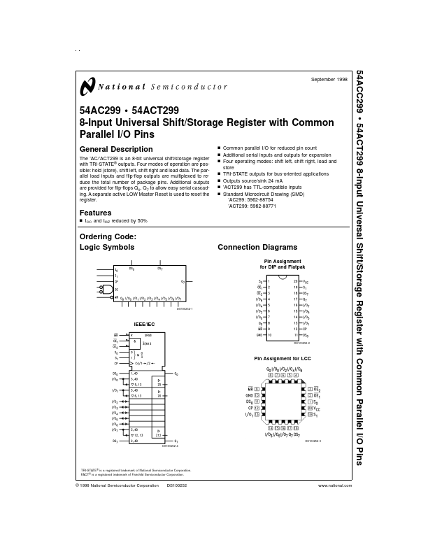
Ordering Code: Logic Symbols
Connection Diagrams
Pin Assignment for DIP and Flatpak
DS100252-1
IEEE/IEC
DS100252-2
Pin Assignment for LCC
DS100252-3 DS100252-4
TRI-STATE ® is a registered trademark of National Semiconductor Corporation. FACT ® is a registered trademark of Fairchild Semiconductor Corporation.
© 1998 National Semiconductor Corporation
DS100252
.national.
Connection Diagrams
Pin Names CP DS0 DS7 S0, S1 MR OE1, OE2 I/O0- I/O7 Q0, Q7
(Continued) Description
Clock Pulse Input Serial Data Input for Right Shift Serial Data Input for Left Shift Mode Select Inputs Asynchronous Master Reset TRI-STATE Output Enable Inputs Parallel Data Inputs or TRI-STATE Parallel Outputs Serial Outputs
Functional Description
The ’AC/’ACT299 contains eight edge-triggered D-type flip-flops and the interstage logic necessary to perform synchronous shift left, shift right, parallel load and hold operations. The type of operation is determined by S0 and S1, as shown in the Truth Table. All flip-flop outputs are brought out through TRI-STATE buffers to separate I/O pins that also serve as data inputs in the parallel load mode. Q0 and Q7 are also...