54F377
54F377 is Octal D Flip-Flop manufactured by National Semiconductor.
Description
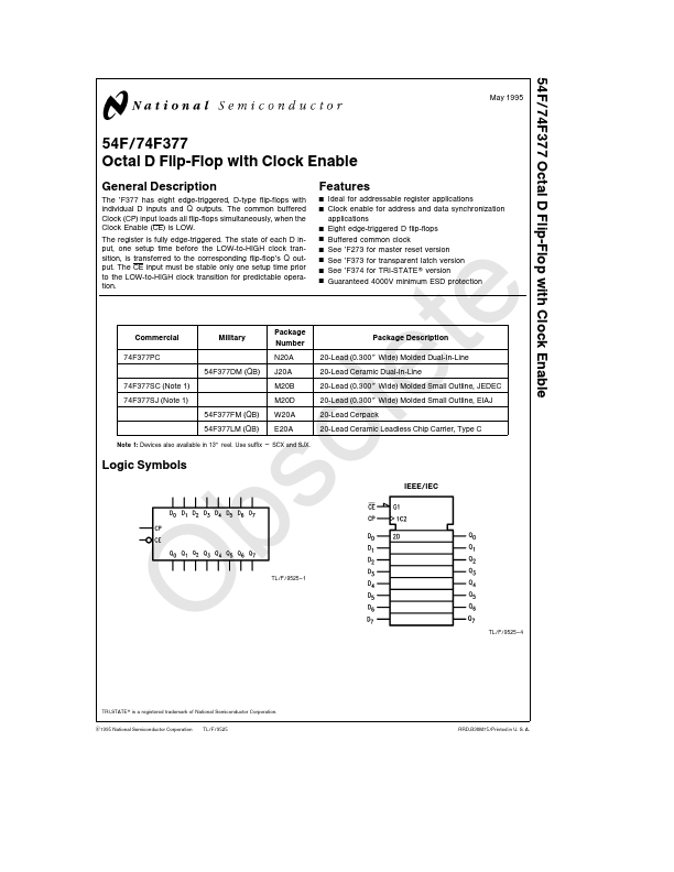
The ’F377 has eight edge-triggered D-type flip-flops with individual D inputs and Q outputs The mon buffered Clock (CP) input loads all flip-flops simultaneously when the Clock Enable (CE) is LOW
The register is fully edge-triggered The state of each D input one setup time before the LOW-to-HIGH clock transition is transferred to the corresponding flip-flop’s Q output The CE input must be stable only one setup time prior to the LOW-to-HIGH clock transition for predictable operation
Features
Y Ideal for addressable register applications Y Clock enable for address and data synchronization applications Y Eight edge-triggered D flip-flops Y Buffered mon clock Y See ’F273 for master reset version Y See ’F373 for transparent latch version Y See ’F374 for TRI-STATE version Y Guaranteed 4000V minimum ESD protection mercial 74F377PC
74F377SC (Note 1) 74F377SJ (Note 1)
Military 54F377DM (QB)
54F377FM (QB) 54F377LM (QB)
Package Number N20A J20A M20B M20D W20A E20A
Package Description
20-Lead (0 300 Wide) Molded Dual-In-Line 20-Lead Ceramic Dual-In-Line 20-Lead (0 300 Wide) Molded Small Outline JEDEC 20-Lead (0 300 Wide) Molded Small Outline EIAJ 20-Lead Cerpack 20-Lead Ceramic Leadless Chip Carrier Type C
Note 1 Devices also available in 13 reel Use suffix e SCX and SJX
Logic Symbols
IEEE IEC
TL F 9525
- 1
TRI-STATE is a registered trademark of National Semiconductor Corporation C1995 National Semiconductor Corporation TL F 9525
TL F 9525
- 4 RRD-B30M75 Printed in U S A
Obsolete
Connection Diagrams
Pin Assignment for DIP SOIC and Flatpak
Pin Assignment for LCC
Unit Loading Fan Out
Pin Names
Description
D0
- D7 CE CP Q0
- Q7
Data Inputs Clock Enable (Active LOW) Clock Pulse Input Data Outputs
TL F 9525- 2
54F 74F
UL HIGH LOW
10 10 10 10 10 10 50 33 3
Input IIH IIL Output IOH IOL
20 m A b0 6 m A 20 m A b0 6 m A 20 m A b0 6 m A b1 m A 20 m A
Operating Mode
Load ‘‘1’’ Load ‘‘0’’ Hold (Do Nothing)
Mode Select-Function Table
Inputs CP CE LI LI Lh...