Description
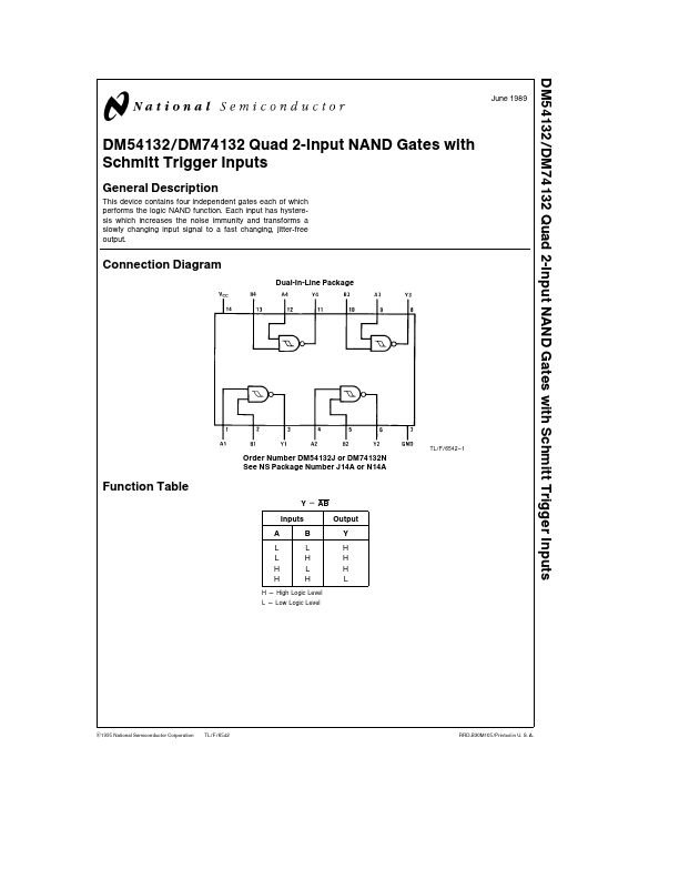
This device contains four independent gates each of which performs the logic NAND function Each input has hysteresis which increases the noise immunity and transforms a slowly changing input signal to a fast changing jitter-free output Connection Diagram Dual-In-Line Package Function Table Order Number DM54132J or DM74132N See NS Package Number J14A or N14A Y e AB Inputs Output AB LL LH HL HH Y H H H L H e High Logic Level L e Low Logic Level TL F 6542 – 1 C1995 National Semiconductor Corporation TL F 6542 RRD-B30M105 Printed in U S A If Military Aerospace specified devices are required please contact the National Semiconductor Sales Office Distributors for availability and specifications Supply Voltage 7V Input Voltage 5 5V Operating Free Air Temperature Range DM54 b55 C to a125 C DM74 0 C to a70 C Storage Temperature Range b65 C to a150 C Note The ‘‘ Remended Operating Conditions Symbol VCC VTa VTb HYS IOH IOL TA Parameter Supply Voltage Positive-Going Input Threshold Voltage (Note 1) Negative-Going Input Threshold Voltage (Note 1) Input Hysteresis (Note 1) High Level Output Current Low Level Output Current Free Air Operating Temperature DM54132 Min Typ Max 45 5 55 15 17 2 06 09 11 04 08 b0 8 16 b55 125 DM74132 Min Typ Max 4 75 5 5 25 15 17 2 06 09 11 04 08 b0 8 16 0 70 Units V V V V mA mA C Symbol Parameter Conditions VI VOH VOL ITa ITb II IIH IIL IOS Input Clamp Voltage High Level Output Voltage Low Level Output Voltage Input Current at Positive-Going Threshold Input Current at Negative-Going Threshold Input Current Max Input Voltage High Level Input Current Low Level Input Current Short Circuit Output Current VCC e Min II e b12 mA VCC e Min IOH e Max VI e VTbMin VCC e Min IOL e Max VI e VTaMax VCC e 5V VI e VTa VCC e 5V VI e VTb VCC e Max VI e 5 5V VCC e Max VI e 2 4V VCC e Max VI e 0 4V VCC e Max (Note 3) ICCH Supply Current with Outputs High VCC e Max ICCL Supply Current with Outputs Low VCC e Max Note 1 VCC e 5V Note 2 All typicals are at VCC e 5V TA e 25 C Note 3 Not more than one output should be shorted at a time DM54 DM74 DM54 DM74 Min 24 24 b18 b18 Typ (Note 2) 34 34 02 b0 43 b0 56 b0 8 15 26 Max b1 5 04 1 40 b1 2 b55 b55 24 40 Units V V V mA mA mA mA mA mA mA mA 2 Switching Characteristics at VCC e 5V and TA e 25 C (See Section 1 for Test Waveforms and Output Load) Symbol Parameter RL e 400X CL e 15 pF Units Min Max tPLH Propagation Delay Time Low to High Level Output 22 ns tPHL Propagation Delay Time High to Low Level Output 22 ns Physical Dimensions inches (millimeters) 14-Lead Ceramic Dual-In-Line Package (J) Order Number DM54132J NS Package Number J14A 3 DM54132 DM74132 Quad 2-Input NAND Gates with Schmitt Trigger Inputs Physical Dimensions inches (millimeters) (Continued) 14-Lead Molded Dual-In-Line Package (N) Order Number DM74132N NS Package Number N14A LIFE SUPPORT POLICY NATIONAL’S PRODUCTS ARE NOT AUTHORIZED FOR USE AS CRITICAL PONENTS IN LIFE SUPPORT DEVICES OR SYSTEMS WITHOUT THE EXPRESS WRITTEN APPROVAL OF THE PRESIDENT OF NATIONAL SEMICONDUCTOR CORPORATION As used herein 1 Life support devices or systems are devices or systems which (a) are intended for surgical implant into the body or (b) support or sustain life and whose failure to pe.