Datasheet Summary
CGS74C2525 CGS74CT2525 CGS74C2526 CGS74CT2526 1-to-8 Minimum Skew Clock Driver
September 1995
CGS74C2525 CGS74CT2525 CGS74C2526 CGS74CT2526 1-to-8 Minimum Skew Clock Driver
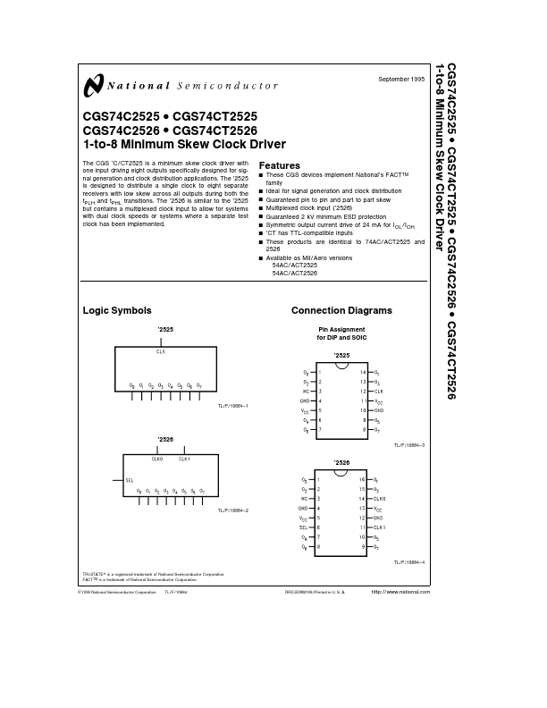
The CGS ’C CT2525 is a minimum skew clock driver with one input driving eight outputs specifically designed for signal generation and clock distribution applications The ’2525 is designed to distribute a single clock to eight separate receivers with low skew across all outputs during both the tPLH and tPHL transitions The ’2526 is similar to the ’2525 but contains a multiplexed clock input to allow for systems with dual clock speeds or systems where a separate test clock has been implemented
Features...