GENERAL DESCRIPTION
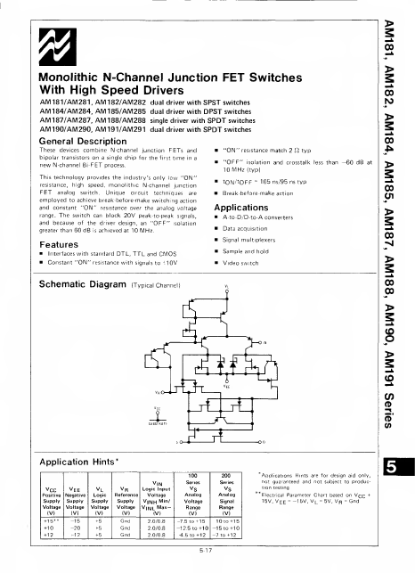
These devices combine N-channel junction FETs and bipolar transistors on a single chip for the first time in a new N-channel Bi-FET process. Unique circuit techniques are employed to achieve break-before-make switching action and constant "ON" resistance over the analog voltage range. FEATURES
Interfaces with standard DTL, TTL and CMOS Constant "ON" resistance with signals to i10V 00 "ON" resistance match 2 i~l typ "OFF" isolation and crosstalk less than —60 dB at 10 MHz (typ) tON'tOFF = 105 ns/95 ns typ 00 Break-before-make action Ol APPLICATIONS
A-to-D/D-to-A converters Data acquisition 00 Signal multiplexers Sample and hold Video switch Schematic Diagram (Typical channe 00 00 o Application Hints* Vcc Positive Supply Voltage (VI + 15" +10 +12 VEE Negative Supply Voltage (V) -15 -20 -12 vL Logic Supply Voltage (V) +5 +5 +5 V|N vR Logic Input Reference Voltage Supply V, NH Mini Voltage V|NL Ma *- (VI (V) Gnd 2.0/0.8 Grid 2.0/0.8 Gnd 2.0/0.8 100 200 Series vS Analog... National Semiconductor