National Semiconductor CD4019BC
CD4019BC is a complementary MOS quad AND-OR select gate Low power and high noise margin over a wide voltage range is possible through implementation of N- and P-channel enhancement mode transistors These complementary MOS (CMOS) transistors provide the building blocks for the 4 ‘‘AND-OR select’’ gate configurations each consisting of two 2-input AND gates driving a single 2-input OR gate Selection is accomplished by control bits KA and KB All inputs are protected against static discharge damage Features Y Y Y Wide supply voltage range High noise immunity Low power TTL compatibility 3 0V to...| Part No. | CD4019BC |
|---|---|
| Datasheet | CD4019BC Download |
| Manufacturer |  National Semiconductor |
| Description | Quad AND-OR Select Gate |
| Buy | Stock & Price |
GENERAL DESCRIPTION
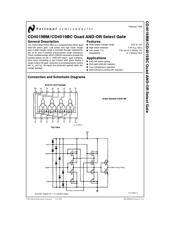
The CD4019BM CD4019BC is a complementary MOS quad AND-OR select gate Low power and high noise margin over a wide voltage range is possible through implementation of N- and P-channel enhancement mode transistors These complementary MOS (CMOS) transistors provide the building blocks for the 4 ‘‘AND-OR select’’ gate configurations each consisting of two 2-input AND gates driving a single 2-input OR gate Selection is accomplished by control bits KA and KB All inputs are protected against static discharge damageFEATURES
Y Y Y Wide supply voltage range High noise immunity Low power TTL compatibility 3 0V to 15V 0 45 VDD (typ ) Fan out of 2 driving 74L or 1 driving 74LSAPPLICATIONS
Y Y Y Y AND-OR select gating Shift-right shift-left registers True complement selection AND OR EXCLUSIVE-OR selection Connection and Schematic Diagrams Dual-In-Line Package Order Number CD4019B TL F 5952 – 1 Top View Schematic diagram for 1 of 4 identical stages C1995 National Semiconductor Co...
