CGS54C2525
CGS54C2525 is 1-to-8 Minimum Skew Clock Driver manufactured by National Semiconductor.
- Part of the CGS74CT2526 comparator family.
- Part of the CGS74CT2526 comparator family.
CGS74C2525 CGS74CT2525 CGS74C2526 CGS74CT2526
1-to-8 Minimum Skew Clock Driver
September 1995
CGS74C2525 CGS74CT2525 CGS74C2526 CGS74CT2526
1-to-8 Minimum Skew Clock Driver
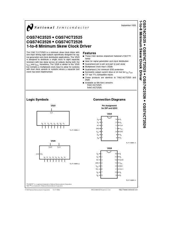
The CGS ’C CT2525 is a minimum skew clock driver with one input driving eight outputs specifically designed for signal generation and clock distribution applications The ’2525 is designed to distribute a single clock to eight separate receivers with low skew across all outputs during both the t PLH and t PHL transitions The ’2526 is similar to the ’2525 but contains a multiplexed clock input to allow for systems with dual clock speeds or systems where a separate test clock has been implemented
Features
Y These CGS devices implement National’s FACTTM family
Y Ideal for signal generation and clock distribution Y Guaranteed pin to pin and part to part skew Y Multiplexed clock input (’2526) Y Guaranteed 2 k V minimum ESD protection Y Symmetric output current drive of 24 m A for IOL IOH Y ’CT has TTL-patible inputs Y These products are identical to 74AC ACT2525 and
2526 Y Available as Mil Aero versions
54AC ACT2525 54AC ACT2526
Logic Symbols
’2525
Connection Diagrams
Pin Assignment for DIP and SOIC
’2525
’2526
TL F 10684
- 1
TL F 10684
- 2
’2526
TL F 10684
- 3
TRI-STATE is a registered trademark of National Semiconductor Corporation FACTTM is a trademark of National Semiconductor Corporation
C1996 National Semiconductor Corporation TL F 10684
RRD-B30M106 Printed in U S A
TL F 10684
- 4 http national
Functional...