Datasheet4U Logo Datasheet4U.com

CGS64B2529 - 1 to 10 Minimum Skew Clock Driver

Download the CGS64B2529 datasheet PDF. This datasheet also covers the CGS6482529 variant, as both devices belong to the same 1 to 10 minimum skew clock driver family and are provided as variant models within a single manufacturer datasheet.

General Description

This minimum skew clock driver is designed for Clock Gen

eration and Support (CGS) applications operating from 33 MHz to 80 MHz.

The devices guarantee minimum output skew across the outputs of a given device.

Key Features

  • Clock Generation and Support (CGS) devices.
  • Ideal for high frequency signal generation or clock distribution.

📥 Download Datasheet

Note: The manufacturer provides a single datasheet file (CGS6482529-NationalSemiconductor.pdf) that lists specifications for multiple related part numbers.

Full PDF Text Transcription (Reference)

The following content is an automatically extracted verbatim text from the original manufacturer datasheet and is provided for reference purposes only.

View original datasheet text
~~ NaStemiicoonnduactlor PRELIMINARY CGS64/7482529 550 ps 1 to 10 Minimum Skew Clock Driver
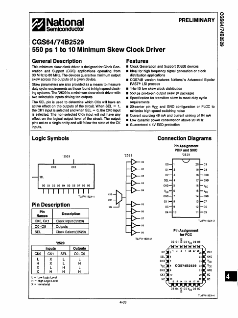
 General Description This minimum skew clock driver is designed for Clock Gen· eration and Support (CGS) applications operating from 33 MHz to 80 MHz. The devices guarantee minimum output skew across the outputs of a given device. Skew parameters are also provided as a means to measure duty cycle requirements as those found in high speed clock· ing systems. The '2529 is a minimum skew clock driver with two selectable inputs driving ten outputs The SEL pin is used to determine which CKn will have an active effect on the outputs of the circuit. When SEL = 1, the CK1 input is selected and when SEL = 0, the CKO input is selected.