Datasheet Summary
CLC109 Low-Power, Wideband, Closed-Loop Buffer
June 1999
CLC109 Low-Power, Wideband, Closed-Loop Buffer
General Description
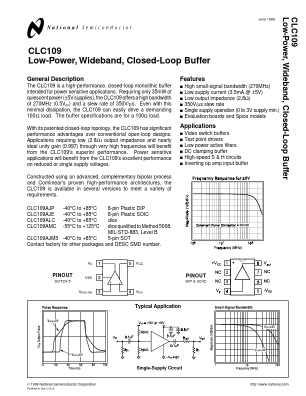
The CLC109 is a high-performance, closed-loop monolithic buffer intended for power sensitive applications. Requiring only 35mW of quiescent power (±5V supplies), the CLC109 offers a high bandwidth of 270MHz (0.5Vpp) and a slew rate of 350V/µs. Even with this minimal dissipation, the CLC109 can easily drive a demanding 100 Ω load. The buffer specifications are for a 100Ω load. With its patented closed-loop topology, the CLC109 has significant performance advantages over conventional open-loop designs. Applications requiring low (2.8Ω) output impedance and nearly...