• Part: CLC5955
  • Description: Broadband Monolithic A/D Converter
  • Manufacturer: National Semiconductor
  • Size: 248.07 KB
Download CLC5955 Datasheet PDF
National Semiconductor
CLC5955
CLC5955 is Broadband Monolithic A/D Converter manufactured by National Semiconductor.
.. April 2002 CLC5955 11-bit, 55MSPS Broadband Monolithic A/D Converter CLC5955 11-bit, 55MSPS Broadband Monolithic A/D Converter General Description 
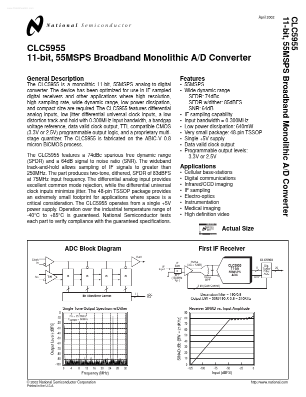
The CLC5955 is a monolithic 11-bit, 55MSPS analog-to-digital converter. The device has been optimized for use in IF-sampled digital receivers and other applications where high resolution, high sampling rate, wide dynamic range, low power dissipation, and pact size are required. The CLC5955 Features differential analog inputs, low jitter differential universal clock inputs, a low distortion track-and-hold with 0-300MHz input bandwidth, a bandgap voltage reference, data valid clock output, TTL patible CMOS (3.3V or 2.5V) programmable output logic, and a proprietary multistage quantizer. The CLC5955 is fabricated on the ABIC-V 0.8 micron Bi CMOS process. The CLC5955 Features a 74d Bc spurious free dynamic range (SFDR) and a 64d B signal to noise ratio (SNR). The wideband track-and-hold allows sampling of IF signals to greater than 250MHz. The part produces two-tone, dithered, SFDR of 83d BFS at 75MHz input frequency. The differential analog input provides excellent mon mode rejection, while the differential universal clock inputs minimize jitter. The 48-pin TSSOP package provides an extremely small footprint for applications where space is a critical consideration. The CLC5955 operates from a single +5V power supply. Operation over the industrial temperature range of -40°C to +85°C is guaranteed. National Semiconductor tests each part to verify pliance with the guaranteed specifications. Features - 55MSPS - Wide dynamic range SFDR: 74d Bc SFDR w/dither: 85d BFS SNR: 64d B - IF sampling capability - Input bandwidth = 0-300MHz - Low power dissipation: 640m W - Very small package: 48-pin TSSOP - Single +5V supply - Data valid clock output - Programmable output levels: 3.3V or 2.5V Applications - - - - - - - - Cellular base-stations Digital munications Infrared/CCD imaging IF sampling...