Description
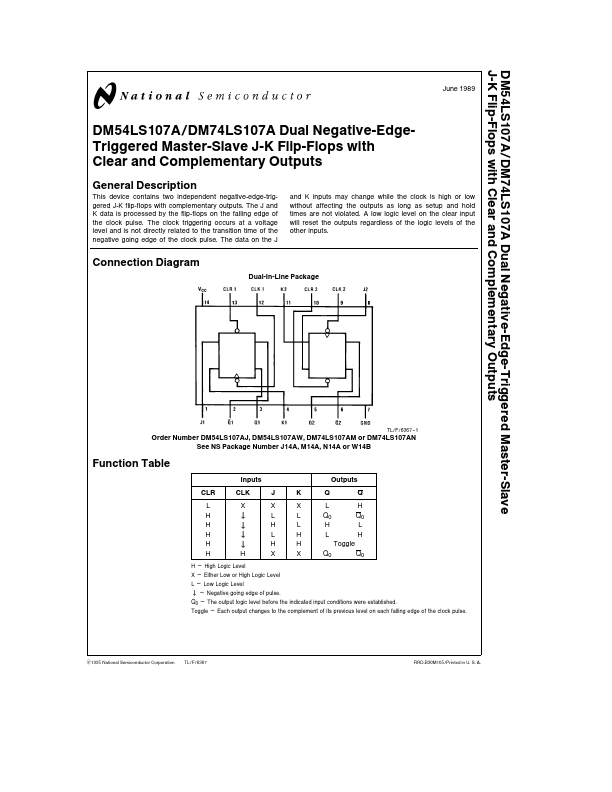
This device contains two independent negative-edge-triggered J-K flip-flops with plementary outputs The J and K data is processed by the flip-flops on the falling edge of the clock pulse The clock triggering occurs at a voltage level and is not directly related to the transition time of the negative going edge of the clock pulse The data on the J and K inputs may change while the clock is high or low without affecting the outputs as long as setup and hold times are not violated A low logic level on the clear input will reset the outputs regardless of the logic levels of the other inputs Connection Diagram Dual-In-Line Package TL F 6367 - 1 Order Number DM54LS107AJ DM54LS107AW DM74LS107AM or DM74LS107AN See NS Package Number J14A M14A N14A or W14B Function Table Inputs CLR L H H H H H CLK X J X L H L H X K X L L H H X Q L Q0 H L Toggle Q0 Q0 Outputs Q H Q0 L H v v v v H H e High Logic Level X e Either Low or High Logic Level L e Low Logic Level v e Negative going edge of pulse Q0 e The output logic level before the indicated input conditions were established Toggle e Each output changes to the plement of its previous level on each falling edge of the clock pulse C1995 National Semiconductor Corporation TL F 6367 RRD-B30M105 Printed in U S A If Military Aerospace specified devices are required please contact the National Semiconductor Sales Office Distributors for availability and specifications Supply Voltage 7V Input Voltage 7V Operating Free Air Temperature Range b 55 C to a 125 C DM54LS DM74LS 0 C to a 70 C b 65 C to a 150 C Storage Temperature Range Note The ‘‘ Remended Operating Conditions Symbol VCC VIH VIL IOH IOL fCLK fCLK tW tW tSU tSU tH tH TA Parameter Min Supply Voltage High Level Input Voltage Low Level Input Voltage High Level Output Current Low Level Output Current Clock Frequency (Note 2) Clock Frequency (Note 3) Pulse Width (Note 2) Pulse Width (Note 3) Setup Time (Notes 1 Setup Time (Notes 1 Hold Time (Notes 1 Hold Time (Notes 1 Clock High Clear Low Clock High Clear Low 2) 3) 2) 3) 0 0 20 25 25 30 20v 25v 0v 5v b 55 DM54LS107A Nom 5 Max 55 Min 4 75 2 07 b0 4 DM74LS107A Nom 5 Max 5 25 Units V V 08 b0 4 45 2 V mA mA MHz MHz ns 4 30 25 0 0 20 25 25 30 20v 25v 0v 5v 125 0 8 30 25 ns ns ns ns ns 70 C Free Air Operating Temperature Note 1 The symbol ( v) indicates the falling edge of the clock pulse is used for reference Note 2 CL e 15 pF RL e 2 kX TA e 25 C and VCC e 5V Note 3 CL e 50 pF RL e 2 kX TA e 25 C and VCC e 5V Symbol VI VOH Parameter Input Clamp Voltage High Level Output Voltage Low Level Output Voltage Conditions VCC e Min II e b18 mA VCC e Min IOH e Max VIL e Max VIH e Min VCC e Min IOL e Max VIL e Max VIH e Min IOL e 4mA VCC e Min II Input Current Input Voltage Max VCC e Max VI e 7V DM54 DM74 DM54 DM74 DM74 J K Clear Clock 25 27 34 34 0 25 0 35 0 25 04 05 04 01 03 04 mA V Min Typ (Note 1) Max b1 5 Units V V VOL 2 over remended operating free air temperature range (unless otherwise noted) (Continued) Symbol IIH Parameter High Level Input Current Conditions VCC e Max VI e 2 7V J K Clear Clock IIL Low Level Input Current VCC e Max VI e 0 4V J K Clear Clock IOS ICC Short Cir.