Description
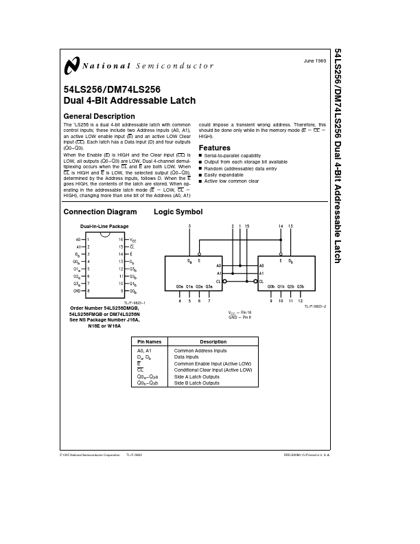
The ’LS256 is a dual 4-bit addressable latch with mon control inputs these include two Address inputs (A0 A1) an active LOW enable input (E) and an active LOW Clear input (CL) Each latch has a Data input (D) and four outputs (Q0 - Q3) When the Enable (E) is HIGH and the Clear input (CL) is LOW all outputs (Q0-Q3) are LOW Dual 4-channel demultiplexing occurs when the CL and E are both LOW When CL is HIGH and E is LOW the selected output (Q0 - Q3) determined by the Address inputs follows D When the E goes HIGH the contents of the latch are stored When operating in the addressable latch mode (E e LOW CL e HIGH) changing more than one bit of the Address (A0 A1) could impose a transient wrong address Therefore this should be done only while in the memory mode (E e CL e HIGH).