DP8420V
DP8420V is microCMOS Programmable 256k/1M/4M Dynamic RAM Controller/Drivers manufactured by National Semiconductor.
- Part of the DP84T22 comparator family.
- Part of the DP84T22 comparator family.
Description
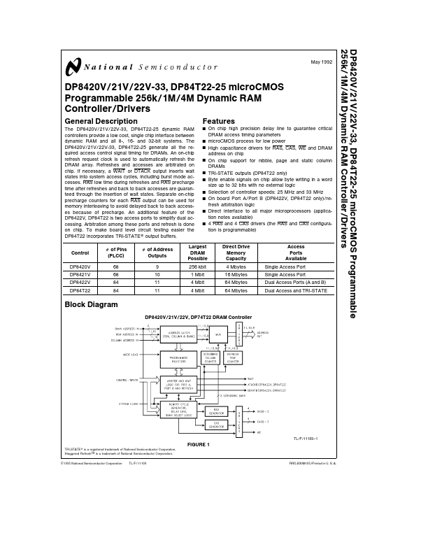
The DP8420V 21V 22V-33 DP84T22-25 dynamic RAM controllers provide a low cost single chip interface between dynamic RAM and all 8- 16- and 32-bit systems The DP8420V 21V 22V-33 DP84T22-25 generate all the required access control signal timing for DRAMs An on-chip refresh request clock is used to automatically refresh the DRAM array Refreshes and accesses are arbitrated on chip If necessary a WAIT or DTACK output inserts wait states into system access cycles including burst mode accesses RAS low time during refreshes and RAS precharge time after refreshes and back to back accesses are guaranteed through the insertion of wait states Separate on-chip precharge counters for each RAS output can be used for memory interleaving to avoid delayed back to back accesses because of precharge An additional feature of the DP8422V DP84T22 is two access ports to simplify dual accessing Arbitration among these ports and refresh is done on chip To make board level circuit testing easier the DP84T22 incorporates TRI-STATE output buffers Control DP8420V DP8421V DP8422V DP84T22 of Pins (PLCC) 68 68 84 84 of Address Outputs 9 10 11 11
Features
On chip high precision delay line to guarantee critical DRAM access timing parameters micro CMOS process for low power High capacitance drivers for RAS CAS WE and DRAM address on chip On chip support for nibble page and static column DRAMs TRI-STATE outputs (DP84T22 only) Byte enable signals on chip allow byte writing in a word size up to 32 bits with no external logic Selection of controller speeds 25 MHz and 33 MHz On board Port A Port B (DP8422V DP84T22 only) refresh arbitration logic Direct interface to all major microprocessors (application notes available) 4 RAS and 4 CAS drivers (the RAS and CAS configuration is programmable)
Largest DRAM Possible 256 kbit 1 Mbit 4 Mbit 4 Mbit
Direct Drive Memory Capacity 4 Mbytes 16 Mbytes 64 Mbytes 64 Mbytes
Access Ports Available Single Access Port Single Access...