DP84910
DP84910 is Integrated Read Channel manufactured by National Semiconductor.
Description
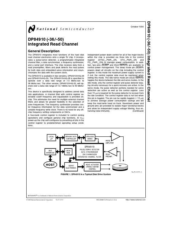
The DP84910 integrates most functions of the hard disk read channel electronics onto a single 5V chip It incorporates a pulse servo detector a programmable integrated channel filter a data synchronizer a frequency synthesizer and a serial port interface The chip receives data from a read preamplifier filters and peak detects the read pulses for both data and embedded servo information and resynchronizes the data with the system clock The DP84910 is available in two versions DP84910VHG-36 and DP84910VHG-50 The DP84910VHG-36 is specified to operate over a data rate range of 7 5 Mbits sec to 36 Mbits sec The other version DP84910VHG-50 will operate over a data rate range of 13 7 Mbits sec to 50 Mbits sec This device is specifically designed to address zoned data rate applications A channel filter with control register selectable cutoff frequency and equalization is provided onchip This eliminates the need for multiple external channel filters and allows for greater flexibility in the selection of zone frequencies The frequency synthesizer provides center frequency information for the data synchronizer and a variable frequency write clock There is no need for any offchip frequency setting ponents or DACs A four-bank control register is included to control zoning operations and configure general chip functions At VCC power-up the chip self-configures by presetting all bits in the control register to predetermined operating setup conditions Independent power down control for all of the major blocks within the chip is provided via three bits in the control register (SYNC PWR DN STH PWR DN and PD PWR DN) to manage power consumption In addition two pins (SLEEP and IDLE SERVO) are available to control power management The sleep mode pin (SLEEP) powers down all circuitry on the chip including the control register In this mode the maximum power supply current is 2 m A the control register data must be reentered when exiting this mode The idle servo mode pin (IDLE...