DS34C86T
DS34C86T is Quad CMOS Differential Line Receiver manufactured by National Semiconductor.
Description
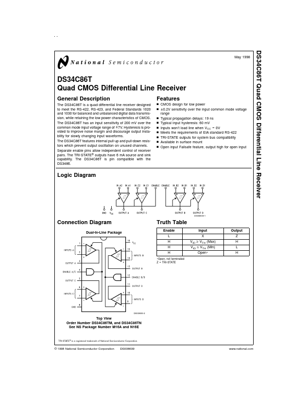
The DS34C86T is a quad differential line receiver designed to meet the RS-422, RS-423, and Federal Standards 1020 and 1030 for balanced and unbalanced digital data transmission, while retaining the low power characteristics of CMOS. The DS34C86T has an input sensitivity of 200 m V over the mon mode input voltage range of ± 7V. Hysteresis is provided to improve noise margin and discourage output instability for slowly changing input waveforms. The DS34C86T features internal pull-up and pull-down resistors which prevent output oscillation on unused channels. Separate enable pins allow independent control of receiver pairs. The TRI-STATE ® outputs have 6 m A source and sink capability. The DS34C86T is pin patible with the DS3486.
Features n CMOS design for low power n ± 0.2V sensitivity over the input mon mode voltage range n Typical propagation delays: 19 ns n Typical input hysteresis: 60 m V n Inputs won’t load line when VCC = 0V n Meets the requirements of EIA standard RS-422 n TRI-STATE outputs for system bus patibility n Available in surface mount n Open input Failsafe feature
, output high for open input
Logic Diagram
DS008699-1
Connection Diagram
Dual-In-Line Package
Truth Table
Enable L H H H
- Open, not terminated Z = TRI-STATE
Input X VID ≥ VTH (Max) VID ≤ VTH (Min) Open-
Output Z H L H
DS008699-2
Top View Order Number DS34C86TM, and DS34C86TN See NS Package Number M16A and N16E
TRI-STATE ® is a registered trademark of National Semiconductor Corporation.
© 1998 National Semiconductor Corporation
DS008699
.national.
Absolute Maximum Ratings (Notes 1, 2)
If Military/Aerospace specified devices are required, please contact the National Semiconductor Sales Office/ Distributors for availability and specifications. Supply Voltage (VCC) Input mon Mode Range (V CM) Differential Input Voltage (V DIFF) Enable Input Voltage (V IN) Storage Temperature Range (T STG) Lead Temperature (Soldering 4 sec) 7V
Maximum Power Dissipation at 25˚C (Note 5)...