DS75365
DS75365 is Quad TTL-to-MOS Driver manufactured by National Semiconductor.
Description
The DS75365 is a quad monolithic integrated TTL-to-MOS driver and interface circuit that accepts standard TTL input signals and provides high-current and high-voltage output levels suitable for driving MOS circuits It is used to drive address control and timing inputs for several types of MOS RAMs including the 1103 The DS75365 operates from the TTL 5V supply and the MOS VSS and VBB supplies in many applications This device has been optimized for operation with VCC2 supply voltage from 16V to 20V and with nominal VCC3 supply voltage from 3V to 4V higher than VCC2 However it is designed so as to be usable over a much wider range of VCC2 and VCC3 In some applications the VCC3 power supply can be eliminated by connecting the VCC3 to the VCC2 pin
Capable of driving high-capacitance loads patible with many popular MOS RAMs Interchangeable with Intel 3207 VCC2 supply voltage variable over side range to 24V maximum VCC3 supply voltage pin available VCC3 pin can be connected to VCC2 pin in some applications TTL patible diode-clamped inputs Operates from standard bipolar and MOS supply voltages Two mon enable inputs per gate-pair High-speed switching Transient overdrive minimizes power dissipation Low standby power dissipation
Features
Quad positive-logic NAND TTL-to-MOS driver Versatile interface circuit for use between TTL and high-current high-voltage systems
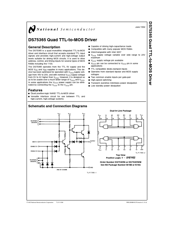
Schematic and Connection Diagrams
Dual-In-Line Package
TL F 7560
- 2
Top View Positive Logic Y e A E1 E2 Order Number DS75365N or DS75365WM See NS Package Number M16B or N16A
TL F 7560
- 1
C1995 National Semiconductor Corporation
TL F 7560
RRD-B30M105 Printed in U S A
Absolute Maximum Ratings (Note 1)
If Military Aerospace specified devices are required please contact the National Semiconductor Sales Office Distributors for availability and specifications Supply Voltage Range of VCC1 Supply Voltage Range of VCC2 Supply Voltage Range of VCC3 nput Voltage...