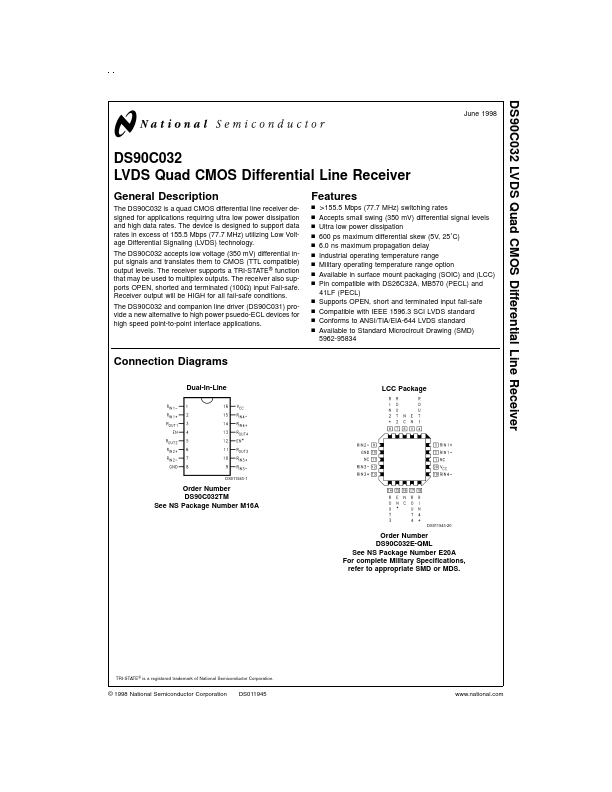
Datasheet4U Logo Datasheet4U.com

DS90C032 - LVDS Quad CMOS Differential Line Receiver

General Description

The DS90C032 is a quad CMOS differential line receiver designed for applications requiring ultra low power dissipation and high data rates.

The device is designed to support data rates in excess of 155.5 Mbps (77.7 MHz) utilizing Low Voltage Differential Signaling (LVDS) technology.

Key Features

  • n n n n n n n n n n n n n > 155.5 Mbps (77.7 MHz) switching rates Accepts small swing (350 mV) differential signal levels Ultra low power dissipation 600 ps maximum differential skew (5V, 25˚C) 6.0 ns maximum propagation delay Industrial operating temperature range Military operating temperature range option Available in surface mount packaging (SOIC) and (LCC) Pin compatible with DS26C32A, MB570 (PECL) and 41LF (PECL) Supports OPEN, short and terminated input fail-safe Compatible with IEEE 159.

📥 Download Datasheet

Full PDF Text Transcription (Reference)

The following content is an automatically extracted verbatim text from the original manufacturer datasheet and is provided for reference purposes only.

View original datasheet text
DS90C032 LVDS Quad CMOS Differential Line Receiver June 1998 DS90C032 LVDS Quad CMOS Differential Line Receiver General Description The DS90C032 is a quad CMOS differential line receiver designed for applications requiring ultra low power dissipation and high data rates. The device is designed to support data rates in excess of 155.5 Mbps (77.7 MHz) utilizing Low Voltage Differential Signaling (LVDS) technology. The DS90C032 accepts low voltage (350 mV) differential input signals and translates them to CMOS (TTL compatible) output levels. The receiver supports a TRI-STATE ® function that may be used to multiplex outputs. The receiver also supports OPEN, shorted and terminated (100Ω) input Fail-safe. Receiver output will be HIGH for all fail-safe conditions.