DS90C032B
Description
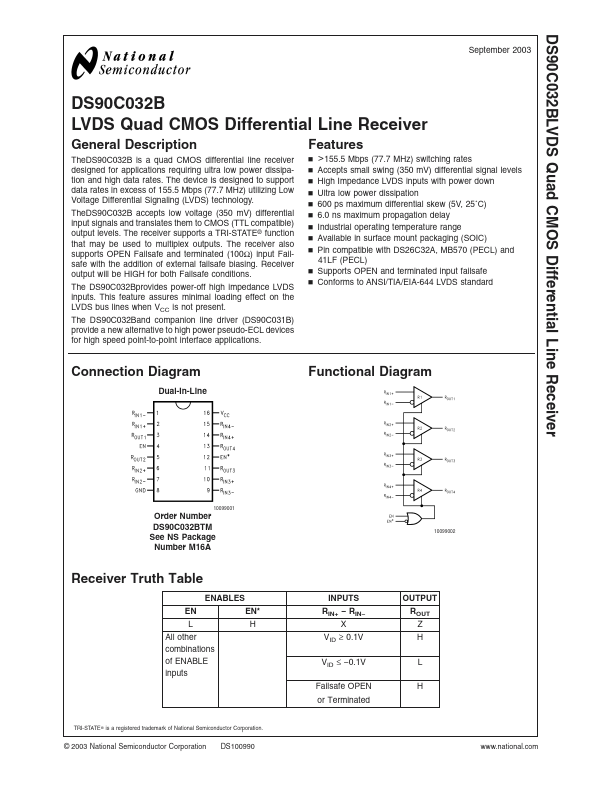
TheDS90C032B is a quad CMOS differential line receiver designed for applications requiring ultra low power dissipation and high data rates.
Key Features
- n >155.5 Mbps (77.7 MHz) switching rates
- Accepts small swing (350 mV) differential signal levels
- High Impedance LVDS inputs with power down
- Ultra low power dissipation n 600 ps maximum differential skew (5V, 25˚C) n 6.0 ns maximum propagation delay
- Industrial operating temperature range
- Available in surface mount packaging (SOIC)
- Supports OPEN and terminated input failsafe
- H L H .national. DS90C032B