DS90CF363
Description
The DS90CF363 transmitter converts 21 bits of CMOS/TTL data into three LVDS (Low Voltage Differential Signaling) data streams.
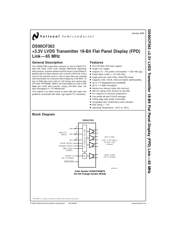
The DS90CF363 transmitter converts 21 bits of CMOS/TTL data into three LVDS (Low Voltage Differential Signaling) data streams.
| Part Number | Manufacturer | Description |
|---|---|---|
| DS90CF363B | Texas Instruments | +3.3V Programmable LVDS Transmitter |
| DS90CF366 | Texas Instruments | 3.3-V LVDS Receiver |
| DS90CF364 | Texas Instruments | +3.3V Programmable LVDS Transmitter |