DS90CF383
Description
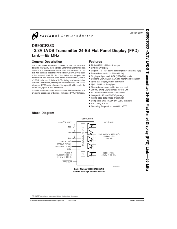
The DS90CF383 transmitter converts 28 bits of CMOS/TTL data into four LVDS (Low Voltage Differential Signaling) data streams.
The DS90CF383 transmitter converts 28 bits of CMOS/TTL data into four LVDS (Low Voltage Differential Signaling) data streams.