DS99R102
Description
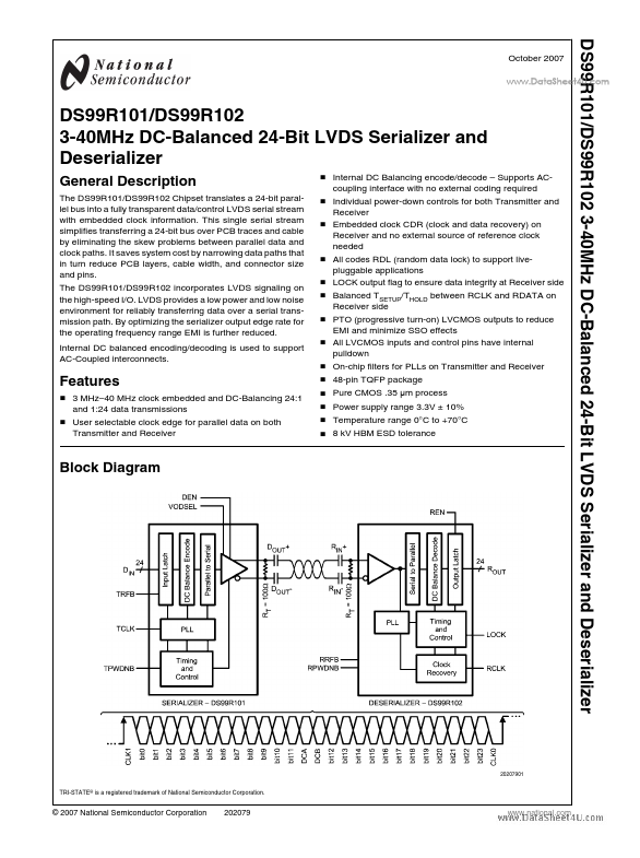
The DS99R101/DS99R102 Chipset translates a 24-bit parallel bus into a fully transparent data/control LVDS serial stream with embedded clock information.
Key Features
- 3 MHz-40 MHz clock embedded and DC-Balancing 24:1 and 1:24 data transmissions Transmitter and Receiver