GENERAL DESCRIPTION
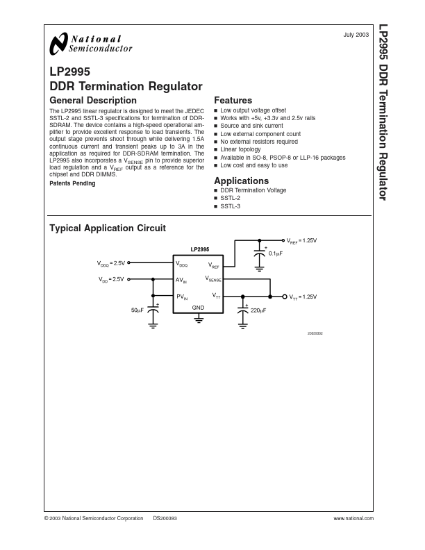
The LP2995 also incorporates a VSENSE pin to provide superior load regulation and a VREF output as a reference for the chipset and DDR DIMMS. Patents Pending FEATURES
n n n n n n n n Low output voltage offset Works with +5v, +3.3v and 2.5v rails Source and sink current Low external component count No external resistors required Linear topology Available in SO-8, PSOP-8 or LLP-16 packages Low cost and easy to use APPLICATIONS
n DDR Termination Voltage n SSTL-2 n SSTL-3 Typical Application Circuit 20039302 © 2003 National Semiconductor Corporation DS200393 LP2995 Connection Diagrams SO-8 (M08A) Package LQA- 16 Package 20039320 Top View 20039304 Top View PSOP-8 (MRA08A) Package 20039350 Top View Pin DESCRIPTION
SO-8 Pin or PSOP-8 Pin 1 2 3 4 5 6 7 8 LLP Pin 1,3,4,6,9, 13,16 2 5 7 8 10 11, 12 14, 15 Name NC GND VSENSE VREF VDDQ AVIN PVIN VTT Function No internal connection. Can be used for vias. Ground. Feedback pin for regulating VTT. Buffered internal reference voltage of VDDQ/2. National Semiconductor