SCAN90CP02
Description
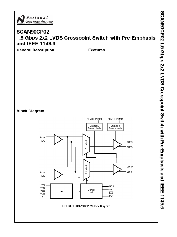
The SCAN90CP02 is a 1.5 Gbps 2 x 2 LVDS crosspoint switch. High speed data paths and flow-through pinout minimize internal device jitter, while configurable 0/25/50/100% pre-emphasis overes external ISI jitter effects of lossy backplanes and cables. The differential inputs interface to LVDS and Bus LVDS signals such as those on National's 10-, 16-, and 18- bit Bus LVDS Ser Des, as well as CML and LVPECL. The SCAN90CP02 can also be used with ASICs and FPGAs. The non-blocking crosspoint architecture is pinconfigurable as a 1:2 clock or data splitter, 2:1 redundancy mux, crossover function, or dual buffer for signal booster and stub hider applications.
Integrated IEEE 1149.1 (JTAG) and 1149.6 circuitry supports testability of both single-ended LVTTL/CMOS and differential LVDS PCB interconnect. The 3.3V supply, CMOS process, and LVDS I/O ensure high performance at low power over the entire industrial -40 to +85°C temperature range.
Features
- 1.5 Gbps per channel
- Low power:...