SCAN90CP02
SCAN90CP02 is 1.5 Gbps 2x2 LVDS Crosspoint Switch manufactured by Texas Instruments.
FEATURES
- 23 1.5 Gbps per channel
- Low power: 70 m A in dual repeater mode @1.5
Gbps
- Low output jitter
- Configurable 0/25/50/100% pre-emphasis drives lossy backplanes and cables
- Non-blocking architecture allows 1:2 splitter,
2:1 mux, crossover, and dual buffer configurations
- Flow-through pinout
- LVDS/BLVDS/CML/LVPECL inputs, LVDS
Outputs
- IEEE 1149.1 and 1149.6 pliant
- Single 3.3V supply
- Separate control of inputs and outputs allows for power savings
- Industrial -40 to +85°C temperature range
- 28-lead LLP package, or 32-lead LQFP package
DESCRIPTION
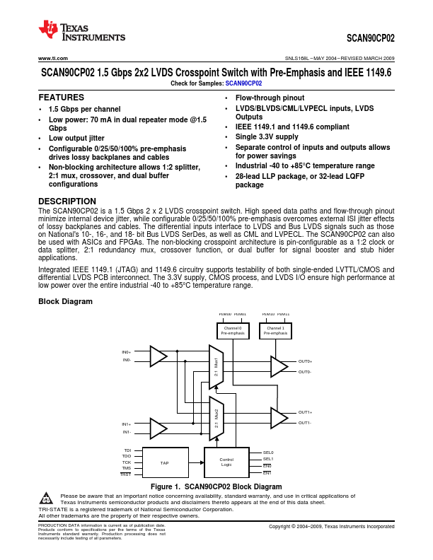
The SCAN90CP02 is a 1.5 Gbps 2 x 2 LVDS crosspoint switch. High speed data paths and flow-through pinout minimize internal device jitter, while configurable 0/25/50/100% pre-emphasis overes external ISI jitter effects of lossy backplanes and cables. The differential inputs interface to LVDS and Bus LVDS signals such as those on National's 10-, 16-, and 18- bit Bus LVDS Ser Des, as well as CML and LVPECL. The SCAN90CP02 can also be used with ASICs and FPGAs. The non-blocking crosspoint architecture is pin-configurable as a 1:2 clock or data splitter, 2:1 redundancy mux, crossover function, or dual buffer for signal booster and stub hider applications.
Integrated IEEE 1149.1 (JTAG) and 1149.6 circuitry supports testability of both single-ended LVTTL/CMOS and differential LVDS PCB interconnect. The 3.3V supply, CMOS process, and LVDS I/O ensure high performance at low power over the entire industrial -40 to +85°C temperature range.
Block Diagram
PEM00 PEM01
PEM10 PEM11
Channel 0 Pre-emphasis
Channel 1 Pre-emphasis
IN0+ IN0-
OUT0+ OUT0-
2:1 Mux1
2:1 Mux2
IN1+ IN1-
OUT1+ OUT1-
TRST
Control Logic
SEL0 SEL1 EN0 EN1
Figure 1. SCAN90CP02 Block...