GENERAL DESCRIPTION
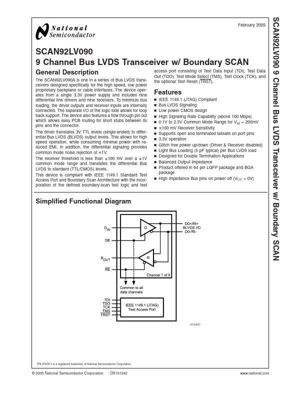
To minimize bus loading, the driver outputs and receiver inputs are internally connected. The device also features a flow through pin out which allows easy PCB routing for short stubs between its pins and the connector. The driver translates 3V TTL levels (single-ended) to differential Bus LVDS (BLVDS) output levels. This allows for high speed operation, while consuming minimal power with reduced EMI. In addition, the differential signaling provides common mode noise rejection of ± 1V. The receiver threshold is less than ± 100 mV over a ± 1V common mode range and translates the differential Bus LVDS to standard (TTL/CMOS) levels. This device is compliant with IEEE 1149.1 Standard Test Access Port and Boundary Scan Architecture with the incorporation of the defined boundary-scan test logic and test access port consisting of Test Data Input (TDI), Test Data Out (TDO), Test Mode Select (TMS), Test Clock (TCK), and the optional Test Reset (TRST). FEATURES
IEEE 1149.1 (J... National Semiconductor