SCAN92LV090
SCAN92LV090 is 9-Channel Bus LVDS Transceiver manufactured by Texas Instruments.
FEATURES
- 2 IEEE 1149.1 (JTAG) pliant
- Bus LVDS Signaling
- Low Power CMOS Design
- High Signaling Rate Capability (Above 100
Mbps)
- 0.1V to 2.3V mon Mode Range for VID =
200m V
- ±100 m V Receiver Sensitivity
- Supports Open and Terminated Failsafe on
Port Pins
- 3.3V Operation
- Glitch Free Power Up/Down (Driver & Receiver
Disabled)
- Light Bus Loading (5 p F Typical) per Bus
LVDS Load
- Designed for Double Termination Applications
- Balanced Output Impedance
- Product Offered in 64 Pin LQFP Package and
NFBGA Package
- High Impedance Bus Pins on Power Off (VCC =
0V)
DESCRIPTION
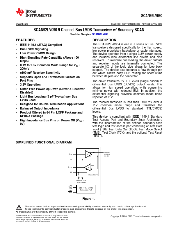
The SCAN92LV090A is one in a series of Bus LVDS transceivers designed specifically for the high speed, low power proprietary backplane or cable interfaces. The device operates from a single 3.3V power supply and includes nine differential line drivers and nine receivers. To minimize bus loading, the driver outputs and receiver inputs are internally connected. The separate I/O of the logic side allows for loop back support. The device also features a flow through pin out which allows easy PCB routing for short stubs between its pins and the connector.
The driver translates 3V TTL levels (single-ended) to differential Bus LVDS (BLVDS) output levels. This allows for high speed operation, while consuming minimal power with reduced EMI. In addition, the differential signaling provides mon mode noise rejection of ±1V.
The receiver threshold is less than ±100 m V over a ±1V mon mode range and translates the differential Bus LVDS to standard (TTL/CMOS) levels.
This device is pliant with IEEE 1149.1 Standard Test Access Port and Boundary Scan Architecture with the incorporation of the defined boundary-scan test logic and test access port consisting of Test Data Input (TDI), Test Data Out (TDO), Test Mode Select (TMS), Test Clock (TCK), and the optional Test Reset (TRST).
SIMPLIFIED FUNCTIONAL DIAGRAM
D0+/RI+ BLVDS I/O D0-/RI-
ROUT RE
R Channel 1 of 9
TDI TDO TCK
TRST mon to...