54AC273
54AC273 is Octal D Flip-Flop manufactured by National Semiconductor.
Description
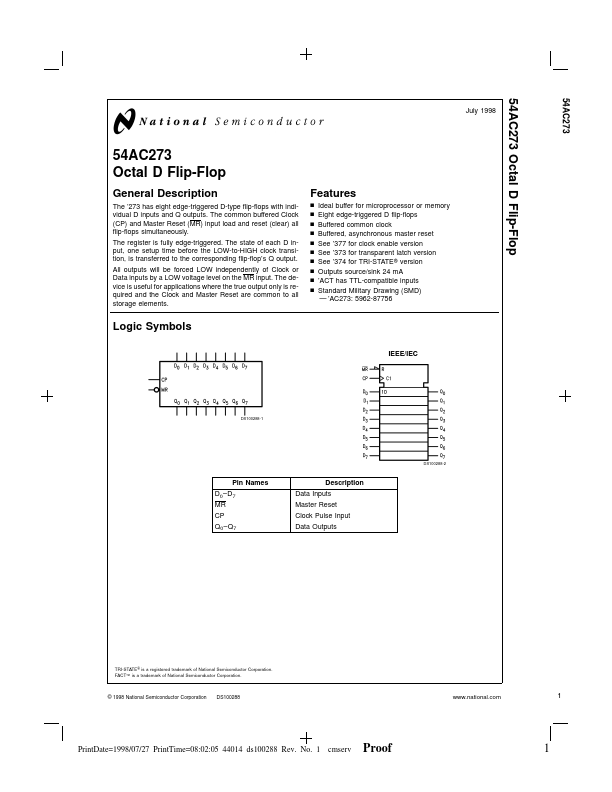
The ’273 has eight edge-triggered D-type flip-flops with individual D inputs and Q outputs. The mon buffered Clock (CP) and Master Reset (MR) input load and reset (clear) all flip-flops simultaneously. The register is fully edge-triggered. The state of each D input, one setup time before the LOW-to-HIGH clock transition, is transferred to the corresponding flip-flop’s Q output. All outputs will be forced LOW independently of Clock or Data inputs by a LOW voltage level on the MR input. The device is useful for applications where the true output only is required and the Clock and Master Reset are mon to all storage elements.
Features n n n n n n n n n n Ideal buffer for microprocessor or memory Eight edge-triggered D flip-flops Buffered mon clock Buffered, asynchronous master reset See ’377 for clock enable version See ’373 for transparent latch version See ’374 for TRI-STATE ® version Outputs source/sink 24 m A ’ACT has TTL-patible inputs Standard Military Drawing (SMD)
- ’AC273: 5962-87756
Logic Symbols
IEEE/IEC
DS100288-1
DS100288-2
Pin Names D0- D7 MR CP Q0- Q7
Description
Data Inputs Master Reset Clock Pulse Input Data Outputs
TRI-STATE ® is a registered trademark of National Semiconductor Corporation. FACT™ is a trademark of National Semiconductor Corporation.
© 1998 National Semiconductor Corporation
DS100288
.national.
Print Date=1998/07/27 Print Time=08:02:05 44014 ds100288 Rev. No. 1 cmserv
Proof
Connection Diagrams
Pin Assignment for DIP and Flatpak Pin Assignment for LCC
DS100288-3 DS100288-4
Mode Select-Function Table
Operating Mode MR Reset (Clear) Load ‘1’ Load ‘0’
H = HIGH Voltage Level L = LOW Voltage Level X = Immaterial N = LOW-to-HIGH Transition
Inputs CP X
Outputs Dn X H L Qn L H L
Logic Diagram
DS100288-5
Please note that this diagram is provided only for the understanding of logic operations and should not be used to estimate propagation delays.
.national.
Print Date=1998/07/27 Print Time=08:02:05...